2024
1215. “Breakdown up to 13.5 kV in NiO/β Ga2O3 Vertical Heterojunction Rectifiers”, Jian Sian Li, Chao Ching Chiang, Hsiao Hsuan Wan, Timothy Jinsoo Yoo, Fan Ren, Honggyu Kim and S.J. Pearton, ECS JSST, 13, 035003 (2024).
1214. “High Sensitivity Saliva Based Biosensor in Detection of Breast Cancer Biomarkers: HER2 and CA15 3”, Hsiao Hsuan Wan, Haochen Zhu, Chao Ching Chiang, Jian Sian Li, Fan Ren, ChenTse Tsai, Yu Te Liao, Josephine F. Esquivel Upshaw and Stephen J. Pearton, Vac. Sci. Technol. B 42, 023202 (2024).
1213. “Effect of Dry Etching to Improve Ohmic Contacts on Bulk, Lightly Doped β Ga2O3“, Chao Ching Chiang, Jian Sian Li, Hsiao Hsuan Wan, Fan Ren and Stephen J. Pearton, ECS JSST 13, 015001 (2024).
1212. “Selective and Non-Selective Plasma Etching of (Al0.18Ga0.82)2O3/ Ga2O3 Heterostructures”, Hsiao-Hsuan Wan, Chao-Ching Chiang, Jian-Sian Li, Fan Ren, Fikadu Alema, Andrei Osinsky and Stephen J. Pearton, J.Vac.Sci. Technol. A 42, 022603 (2024).
1211. “Effect of High Current Density Pulses on Performance Enhancement of Optoelectronic Devices”, Md Hafijur Rahman, Nicholas Glavin, Aman Haque, Fan Ren and Stephen J. Pearton ECS J. Sol. State Sci.Technol. 13, 025003 (2024).
2023
1210. “Reducing proton radiation vulnerability in AlGaN/GaN high electron mobility transistors with residual strain relief”, Nahid Sultan Al Mamun, J. Bae, Jihyun Kim, Aman Haque, Douglas E. Wolfe, Fan Ren and Stephen Pearton, J. Appl. Phys. 134, 224901 (2023).
1209. “E mode AlGaN /GaN HEMTs Using p NiO Gates”, Chao Ching Chiang, Hsiao Hsuan Wan, Jian Sian Li, Fan Ren, Timothy Jinsoo Yoo, Honggyu Kim and S. J. Pearton, J. Vac. Sci. Technol. B 41, 062205 (2023).
1208. “NiO/Ga2O3 Vertical Rectifiers of 7 kV and 1 mm2 with 5.5 A Forward Conduction Current”, Jian Sian Li, Chao Ching Chiang, Hsiao Hsuan Wan, Timothy Jinsoo Yoo, Fan Ren, Honggyu Kim and S.J. Pearton, Crystals 13, 1624 (2023).
1207. “Evaluation of dry stored disposable sensor strip on rapid SARS-CoV-2 detection platform”, Chao-Ching Chiang, Chan-Wen Chiu , Fan Ren , Cheng-Tse Tsai, Yu-Te Liao, Josephine F. Esquivel-Upshaw, Stephen J. Pearton, Vac. Sci. Technol. B41, 012204 (2023).
1206. “Radiation damage in GaN/AlGaN and SiC electronic and photonic devices”, J. Pearton, Xinyi Xia, Fan Ren, Md Abu Jafar Rasel, Sergei Stepanoff, Nahid Al-Mamun, Aman Haque, Douglas E. Wolfe, J. Vac. Sci. Technol. B41, 030802 (2023).
1205. “Sidewall Electrical Damage in β-Ga2O3 Rectifiers Exposed to Ga+ Focused Ion Beams”, Xinyi Xia, Nahid Sultan Al-Mamun, Fan Ren, Aman Haque and J. Pearton, ECS J. Solid State Sci. Technol. 12, 055003 (2023).
1204. “NiO/β-(AlxGa1−x)2O3/Ga2O3 heterojunction lateral rectifiers with reverse breakdown voltage >7 kV”, Hsiao-Hsuan Wan, Jian-Sian Li, Chao-Ching Chiang, Xinyi Xia, Fan Ren, Hannah N. Masten, James Spencer Lundh, Joseph A. Spencer, Fikadu Alema, Andrei Osinsky, Alan G. Jacobs, Karl Hobart, Marko J. Tadjer, J. Pearton, J. Vac. Sci. Technol. A41, 032701 (2023).
1203. “Heavy ion irradiation induced failure of gallium nitride high electron mobility transistors: effects of in-situ biasing”, Md Abu Jafar Rasel, Ryan Schoell, Nahid Sultan Al-Mamun, Khalid Hattar, C Thomas Harris, Aman Haque, Douglas E Wolfe, Fan Ren and Stephen J Pearton, Phys. D: Appl. Phys. 56 305104 (2023).
1202. “The Optimization of NiO Doping, Thickness, and Extension in kV-Class NiO/Ga2O3 Vertical Rectifiers”, Chao-Ching Chiang, Jian-Sian Li, Hsiao-Hsuan Wan, Fan Ren Stephen Pearson, Crystal, 13, 1124 (2023).
1201. “β-Ga2O3 orientation dependence of band offsets with SiO2 and Al2O3”, Hsiao-Hsuan Wan, Jian-Sian Li, Chao-Ching Chiang, Xinyi Xia, David C. Hays, Fan Ren, and Stephen J. Pearton, J. Vac. Sci. Technol. A41, 063250 (2023).
1200. “Properties of SiCN Films Relevant to Dental Implant Applications”, Xinyi Xia, Chao-Ching Chiang, Sarathy K. Gopalakrishnan, Aniruddha V. Kulkarni, Fan Ren, Kirk J. Ziegler, Josephine F. Esquivel-Upshaw, Materials, 16, 5318 (2023).
1199. “1 mm2, 3.6 kV, 4.8 A NiO/Ga2O3 Heterojunction Rectifiers”, Jian-Sian Li, Chao-Ching Chiang, Xinyi Xia, Hsiao-Hsuan Wan, Fan Ren and J. Pearton, ECS J. Solid State Sci. Technol. 12, 085001 (2023).
1198. “Annealing Stability of NiO/Ga2O3 Vertical Heterojunction Rectifiers”, Jian-Sian Li, Hsiao-Hsuan Wan, Chao-Ching Chiang, Fan Ren, Stephen J. Pearton, Crystal 13, 1174 (2023).
1197. “Comparison of 10 MeV Neutron Irradiation Effects on NiO/Ga2O3 Heterojunction Rectifiers and Ni/Au/Ga2O3 Schottky Rectifiers”, Jian-Sian Li, Xinyi Xia, Chao-Ching Chiang, Hsiao-Hsuan Wan, Fan Ren, Jihyun Kim2 and J. Pearton, ECS J. Solid State Sci. Technol. 12, 075004 (2023).
1196. “Superior high temperature performance of 8 kV NiO/Ga2O3 vertical heterojunction rectifiers”, Jian-Sian Li, Chao-Ching Chiang, Xinyi Xia, Hsiao-Hsuan Wan, Fan Ren and J. Pearton, J. Mat. Chem. C, 11, 7750 (2023).
1195. “Reproducible NiO/Ga2O3 Vertical Rectifiers with Breakdown Voltage > 8 kV”, Jian-Sian Li, Hsiao-Hsuan Wan,Chao-Ching Chiang, Xinyi Xia, Yoo, Timothy Jinsoo Kim, Honggyu Kim, Fan Ren, J. Pearton, Crystal, 13, 886 (2023).
1194. “Ion energy dependence of dry etch damage depth in Ga2O3 Schottky rectifiers”, Chao-Ching Chiang, Xinyi Xia, Jian-Sian, Fan Ren, J. Pearton, Appl. Surf. Sci., 631, 157489 (2023).
1193. “Effect of drift layer doping and NiO parameters in achieving 8.9 kV breakdown in 100 μm diameter and 4 kV/4 A in 1 mm diameter NiO/β-Ga2O3 rectifiers”, Jian-Sian Li, Chao-Ching Chiang, Xinyi Xia, Hsiao-Hsuan Wan, Fan Ren and J. Pearton, J. Vac. Sci. Technol. A41, 043404 (2023).
1192. “60Co γ-irradiation of AlGaN UVC light-emitting diodes”, Xinyi Xia,Sergei Stepanoff,Aman Haque,Douglas E. Wolfe, Simon Barke, Peter J. Wass, Fan Ren,John W., S. J. Pearton, Optical Mat., 142, 114015 (2023).
1191. “15 MeV proton damage in NiO/β-Ga2O3 vertical rectifiers”, Jian-Sian Li, Chao-Ching Chiang, Xinyi Xia, Hsiao-Hsuan Wan, Jihyun Kim, Fan Ren and J. Pearton,J. Phys. Mat., 6, 045003 (2023).
1190. “Enhancing the Hydrophobicity and Antibacterial Properties of SiCN-Coated Surfaces with Quaternization to Address Peri-Implantitis”, Chao-Ching Chiang,Xinyi Xia, Valentin Craciun,Rocha Mateus Garcia,Samira Esteves Afonso Camargo, Fernanda Regina Godoy Rocha,Sarathy K.Gopalakrishnan, Kirk J, Ziegler, Fan Ren, Josephine F. Esquivel-Upshaw, Materials, 16, 5751 (2023).
1189. “Rapid detection of radiation susceptible regions in electronics”, Sergei P. Stepanoff,Aman Haque, Fan Ren, Stephen J. Pearton, Douglas E.Wolfe, Vac. Sci. Technol. B41, 044005 (2023).
1188. “Ultrafast, room temperature rejuvenation of SiC Schottky diodes from forward current-induced degradation”, Md Abu Jafar Rasel, Nahid Sultan Al-Mamun,Sergei Stepanoff, AmanHaque, Douglas E. Wolfe, Fan Ren, Stephen J.Pearton, Appl. Phys. Lett., 122, 204101 (2023).
1187. “Operation of NiO/β-(Al21Ga0.79)2O3/Ga2O3 Heterojunction Lateral Rectifiers at up to 225°C”, Hsiao-Hsuan, Jian-Sian Li, Chao-Ching Chiang, Xinyi Xia, Fan Ren, Hannah N. Masten, James Spencer Lundh, Joseph A. Spencer, Fikadu Alema, Andrei Osinsky, Alan G. Jacobs, Karl Hobart, Marko J. Tadjer, S. J. Pearton, ECS J. Solid State Sci. Technol. 12, 075008 (2023).
1186. “Review-Reliability and Degradation Mechanisms of Deep UV AlGaN LEDs”, Benjamin C. Letson, John W. Conklin, Peter Wass, Simon Barke, Guido Mueller, Md Abu C. Jafar Rasel, Aman Haque, S. J. Pearton, Fan Ren, ECS J. Solid State Sci. Technol. 12, 066002 (2023).
1185. “Impact of neutron irradiation on electronic carrier transport properties in Ga2O3 and comparison with proton irradiation effects”, Jonathan Lee, Andrew C. Silverman, Elena Flitsiyan, Minghan Xian, Fan Ren, S. J. Pearton, Radiation Effects & Defects in Solids, 178, 680-689 (2023).
1184. “Vertical NiO/Ga2O3 Rectifiers Grown by Metal Organic Chemical Vapor Deposition”,Hsiao Hsuan Wan, Jian Sian Li, Chao Ching Chiang, Fan Ren, Timothy Jinsoo Yoo, Honggyu Kim, Andrei Osinsky, Fikadu Alema and Stephen J. Pearton, J. Vac. Sci. Technol. A 41, 052707(2023).
1183. “Localized Stress Effects on the Single Event Effects Sensitivity of Microelectronics”, Sergei P. Stepanoff, Ani Khachatrian, Aman Haque, Fan Ren, Stephen Pearton, and Douglas E. Wolfe, Microelectronics (2023).
1182. “Effect of Biased Field Rings to Improve Charge Removal after Heavy-Ion Strikes in Vertical Geometry β-Ga2O3 Rectifiers”, Ribhu Sharma, Jian-Sian Li, Mark E. Law, Fan Ren, and J. Pearton, ECS J. Solid State Sci. Technol. 12, 035003 (2023).
1181. “Evaluation of dry stored disposable sensor strip on rapid SARS-CoV-2 detection platform”, Chao-Ching Chiang, Chan-Wen Chiu , Fan Ren , Cheng-Tse Tsai, Yu-Te Liao, Josephine F. Esquivel-Upshaw, Stephen J. Pearton, Vac. Sci. Technol. B41, 012204 (2023).
1180. “Radiation damage in GaN/AlGaN and SiC electronic and photonic devices”, J. Pearton, Xinyi Xia, Fan Ren, Md Abu Jafar Rasel, Sergei Stepanoff, Nahid Al-Mamun, Aman Haque, Douglas E. Wolfe, J. Vac. Sci. Technol. B41, 030802 (2023).
1179. “Sidewall Electrical Damage in β-Ga2O3 Rectifiers Exposed to Ga+ Focused Ion Beams”, Xinyi Xia, Nahid Sultan Al-Mamun, Fan Ren, Aman Haque and J. Pearton, ECS J. Solid State Sci. Technol. 12, 055003 (2023).
1178. “NiO/β-(AlxGa1−x)2O3/Ga2O3 heterojunction lateral rectifiers with reverse breakdown voltage >7 kV”, Hsiao-Hsuan Wan, Jian-Sian Li, Chao-Ching Chiang, Xinyi Xia, Fan Ren, Hannah N. Masten, James Spencer Lundh, Joseph A. Spencer, Fikadu Alema, Andrei Osinsky, Alan G. Jacobs, Karl Hobart, Marko J. Tadjer, J. Pearton, J. Vac. Sci. Technol. A41, 032701 (2023).
1177. “Heavy ion irradiation induced failure of gallium nitride high electron mobility transistors: effects of in-situ biasing”, Md Abu Jafar Rasel, Ryan Schoell, Nahid Sultan Al-Mamun, Khalid Hattar, C Thomas Harris, Aman Haque, Douglas E Wolfe, Fan Ren and Stephen J Pearton, Phys. D: Appl. Phys. 56 305104 (2023).
1176. “The Optimization of NiO Doping, Thickness, and Extension in kV-Class NiO/Ga2O3 Vertical Rectifiers”, Chao-Ching Chiang, Jian-Sian Li, Hsiao-Hsuan Wan, Fan Ren Stephen Pearson, Crystal, 13, 1124 (2023).
1175. “β-Ga2O3 orientation dependence of band offsets with SiO2 and Al2O3”, Hsiao-Hsuan Wan, Jian-Sian Li, Chao-Ching Chiang, Xinyi Xia, David C. Hays, Fan Ren, and Stephen J. Pearton, J. Vac. Sci. Technol. A41, 063250 (2023).
1174. “Properties of SiCN Films Relevant to Dental Implant Applications”, Xinyi Xia, Chao-Ching Chiang, Sarathy K. Gopalakrishnan, Aniruddha V. Kulkarni, Fan Ren, Kirk J. Ziegler, Josephine F. Esquivel-Upshaw, Materials, 16, 5318 (2023).
1173. “1 mm2, 3.6 kV, 4.8 A NiO/Ga2O3 Heterojunction Rectifiers”, Jian-Sian Li, Chao-Ching Chiang, Xinyi Xia, Hsiao-Hsuan Wan, Fan Ren and J. Pearton, ECS J. Solid State Sci. Technol. 12, 085001 (2023).
1172. “Annealing Stability of NiO/Ga2O3 Vertical Heterojunction Rectifiers”, Jian-Sian Li, Hsiao-Hsuan Wan, Chao-Ching Chiang, Fan Ren, Stephen J. Pearton, Crystal 13, 1174 (2023).
1171. “Comparison of 10 MeV Neutron Irradiation Effects on NiO/Ga2O3 Heterojunction Rectifiers and Ni/Au/Ga2O3 Schottky Rectifiers”, Jian-Sian Li, Xinyi Xia, Chao-Ching Chiang, Hsiao-Hsuan Wan, Fan Ren, Jihyun Kim2 and J. Pearton, ECS J. Solid State Sci. Technol. 12, 075004 (2023).
1170. “Superior high temperature performance of 8 kV NiO/Ga2O3 vertical heterojunction rectifiers”, Jian-Sian Li, Chao-Ching Chiang, Xinyi Xia, Hsiao-Hsuan Wan, Fan Ren and J. Pearton, J. Mat. Chem. C, 11, 7750 (2023).
1169. “Reproducible NiO/Ga2O3 Vertical Rectifiers with Breakdown Voltage; 8 kV”, Jian-Sian Li, Hsiao-Hsuan Wan,Chao-Ching Chiang, Xinyi Xia, Yoo, Timothy Jinsoo Kim, Honggyu Kim, Fan Ren and S. J. Pearton Crystal, 13, 886 (2023).
1168. “Ion energy dependence of dry etch damage depth in Ga2O3 Schottky rectifiers”, Chao-Ching Chiang, Xinyi Xia, Jian-Sian, Fan Ren, J. Pearton, Appl. Surf. Sci., 631, 157489 (2023).
1167. “Effect of drift layer doping and NiO parameters in achieving 8.9 kV breakdown in 100 μm diameter and 4 kV/4 A in 1 mm diameter NiO/β-Ga2O3 rectifiers”, Jian-Sian Li, Chao-Ching Chiang, Xinyi Xia, Hsiao-Hsuan Wan, Fan Ren and J. Pearton, J. Vac. Sci. Technol. A41, 043404 (2023).
1166. “60Co γ-irradiation of AlGaN UVC light-emitting diodes”, Xinyi Xia,Sergei Stepanoff,Aman Haque,Douglas E. Wolfe, Simon Barke, Peter J. Wass, Fan Ren,John W., S. J. Pearton, Optical Mat., 142, 114015 (2023).
1165. “15 MeV proton damage in NiO/β-Ga2O3 vertical rectifiers”, Jian-Sian Li, Chao-Ching Chiang, Xinyi Xia, Hsiao-Hsuan Wan, Jihyun Kim, Fan Ren and J. Pearton,J. Phys. Mat., 6, 045003 (2023).
1164. “Enhancing the Hydrophobicity and Antibacterial Properties of SiCN-Coated Surfaces with Quaternization to Address Peri-Implantitis”, Chao-Ching Chiang,Xinyi Xia, Valentin Craciun,Rocha Mateus Garcia,Samira Esteves Afonso Camargo, Fernanda Regina Godoy Rocha,Sarathy K.Gopalakrishnan, Kirk J, Ziegler, Fan Ren, Josephine F. Esquivel-Upshaw, Materials, 16, 5751 (2023).
1163. “Rapid detection of radiation susceptible regions in electronics”, Sergei P. Stepanoff,Aman Haque, Fan Ren, Fan,Stephen J. Pearton, Douglas E.Wolfe, Vac. Sci. Technol. B41, 044005 (2023).
1162. ”Ultrafast, room temperature rejuvenation of SiC Schottky diodes from forward current-induced degradation”, Md Abu Jafar Rasel, Nahid Sultan Al-Mamun,Sergei Stepanoff, AmanHaque, Douglas E. Wolfe, Fan Ren, Stephen J.Pearton, Appl. Phys. Lett., 122, 204101 (2023).
1161.“Operation of NiO/β-(Al21Ga0.79)2O3/Ga2O3 Heterojunction Lateral Rectifiers at up to 225°C”, Hsiao-Hsuan, Jian-Sian Li, Chao-Ching Chiang, Xinyi Xia, Fan Ren, Hannah N. Masten, James Spencer Lundh, Joseph A. Spencer, Fikadu Alema, Andrei Osinsky, Alan G. Jacobs, Karl Hobart, Marko J. Tadjer, S. J. Pearton, ECS J. Solid State Sci. Technol. 12, 075008 (2023).
1160. “Review-Reliability and Degradation Mechanisms of Deep UV AlGaN LEDs”, Benjamin C. Letson, John W. Conklin, Peter Wass, Simon Barke, Guido Mueller, Md Abu C. Jafar Rasel, Aman Haque, S. J. Pearton, Fan Ren, ECS J. Solid State Sci. Technol. 12, 066002 (2023).
1159. “Impact of neutron irradiation on electronic carrier transport properties in Ga2O3 and comparison with proton irradiation effects”, Jonathan Lee, Andrew C. Silverman, Elena Flitsiyan, Minghan Xian, Fan Ren, S. J. Pearton, Radiation Effects & Defects in Soilids, 178, 680-689 (2023).
1158. “Type-II band alignment for atomic layer deposited HfSiO4 on alpha- Ga2O3”,Xinyi Xia, Jian-Sian Li, Zhuoqun Wen, Kamruzzaman Khan, Md Irfan Khan, Elaheh Ahmadi,
Yuichi Oshima, David C. Hays, Fan Ren, and S. J. Pearton, Vac. Sci. Technol. A41, 023205 (2023).
1157. “7.5 kV, 6.2 GW cm-2 NiO/beta-Ga2O3 vertical rectifiers with on-off ratio greater than 10”, Jian-Sian Li, Chao-Ching Chiang, Xinyi Xia, Hsiao-Hsuan Wan, Fan Ren, S. J. Pearton, J. Vac. Sci. Technol. A41, 030401 (2023).
1156. “Evaluation of dry stored disposable sensor strip on rapid SARS-CoV-2 detection platform”, Chao-Ching Chiang, Chan-Wen Chiu, Fan Ren, Cheng-Tse Tsai, Yu-Te Liao, Josephine F. Esquivel-Upshaw, and Stephen J. Pearton, J. Sci. Technol. B41, 012204 (2023).
1155. “High sensitivity CIP2A detection for oral cancer using a rapid transistor-based biosensor module”, Minghan Xian, Jenna L. Stephany, Chan-Wen Chiu, Chao-Ching Chiang, Fan Ren, Cheng-Tse Tsai, Siang-Sin Shan, Yu-Te Liao, Josephine F. Esquivel-Upshaw, and Stephen J. Pearton, Vac. Sci. Technol. B41, 013201 (2023).
1154. “Deep UV AlGaN LED reliability for long duration space missions”, Benjamin C. Letson, Simon Barke, Peter Wass, Guido Mueller, Fan Ren, Stephen J. Pearton, and John W. Conklin, Vac. Sci. Technol. A41, 013202 (2023).
1153. “Deposition of sputtered NiO as a p-type layer for heterojunction diodes with Ga2O3”, Jian-Sian Li, Xinyi Xia, Chao-Ching Chiang, David C. Hays, Brent P. Gila, Valentin Craciun, Fan Ren, and J. Pearton, J. Vac. Sci. Technol. A41, 013405 (2023).
1152. “Reversible total ionizing dose effects in NiO/Ga2O3 heterojunction rectifiers”, Jian-Sian Li, Chao-Ching Chiang, Xinyi Xia, Sergei Stepanoff, Aman Haque, Douglas E. Wolfe, Fan Ren, and S. J. Pearton, J. Appl. Phys., 133, 015702 (2023).
2022
1151. “Band alignment of sputtered and atomic layer deposited SiO2 and Al2O3 on ScAlN”, Xinyi Xia, Jian-Sian Li, Md Irfan Khan, Kamruzzaman Khan, Elaheh Ahmadi, David C. Hays, Fan Ren, and J. Pearton, J. Appl. Phys., 132, 235791 (2022).
1150. “Analytical Specificity and Microbial Interference Study of a 30-Second Quantitative SARS-CoV-2 Detection Biosensor System”, Chao-Ching Chiang, Chan-Wen Chiu, Fan Ren, Cheng-Tse Tsai, Yu-Te Liao, Josephine F. Esquivel-Upshaw and Stephen J. Pearton, ECS J. Solid State Sci. Technol., 11, 105007 (2022).
1149. “Heuristic Detection of the Most Vulnerable Regions in Electronic Devices for Radiation Survivability”, Stepanoff, Sergei; Rasel, Md; Haque, Aman; Wolfe, Douglas; Ren, Fan; Pearton, Stephen, ECS J. Solid State Sci. Technol., 11, 085008 (2022).
1148. “The Effect of Amino Sugars on the Composition and Metabolism of a Microcosm Biofilm and the Cariogenic Potential against Teeth and Dental Materials”, Lin Zeng, Alejandro Riveros Walker, Patricia dos Santos Calderon, Xinyi Xia, Fan Ren and Josephine F. Esquivel-Upshaw, J. Funct. Biomater., 13, 223 (2022).
1147. “Color perceptibility and validity of silicon carbide-based protective coatings for dental ceramics”, Chaker Fares, Randy Elhassani, Fan Ren, Alexandra R. Cabrera, Ingrid Chai, Dan Neal, Shu-Min Hsu, and Josephine F. Esquive.l-Upshaw, J. Prosth. Dent., 127 918-924 (2022).
1146. “Selective Wet and Dry Etching of NiO over beta-Ga2O3”, Chao-Ching Chiang, Chan-Wen Chiu, Fan Ren, Cheng-Tse Tsai, Yu-Te Liao, Josephine F. Esquivel-Upshaw, and Stephen J. Pearton, Vac. Sci. Technol. B40, 012204 (2022).
1145. “Dynamic Switching of 1.9 A/1.76 kV Forward Current NiO/beta-Ga2O3 Rectifiers”, Jian-Sian Li, Chao-Ching Chiang, Xinyi Xia, Cheng-Tse Tsai, Fan Ren, Yu-Te Liao, and J. Pearton, ECS J. Solid State Sci. Technol., 11, 105003 (2022).
1144. “High volume UV LED performance testing”, Benjamin C. Letson, Simon Barke, Samantha Parry Kenyon, Taiwo Olatunde, Guido Mueller, Peter Wass, Fan Ren, Stephen J. Pearton, and John W. Conklin, Rev. Sci. Instrum., 93, 114503 (2022).
1143. “Fracture of Lithia Disilicate Ceramics under Different Environmental Conditions”, Josephine F. Esquivel-Upshaw,Shu-Min Hsu, Fan Ren, Jenna Stephany, Xinyi Xia, Chan-Wen Chiu, Dan Neal and John J. Mecholsky, Jr., Materials, 15, 155261 (2022).
1142. “Type II band alignment of NiO/alpha-Ga2O3 Ga2O3 for annealing temperatures up to 600°C”, Xinyi Xia, Jian-Sian Li, Chao-Ching Chiang, Timothy Jinsoo Yoo, Eitan Hershkovitz, Fan Ren1, Honggyu Kim, Jihyun Kim, Dae-Woo Jeon, Ji-Hyeon Park, and J. Pearton, J. Vac. Sci. Technol. A40, 063408 (2022).
1141. “Temperature dependence of on-off ratio and reverse recovery time in NiO/beta-Ga2O3 heterojunction rectifiers”, Jian-Sian Li, Chao-Ching Chiang, Xinyi Xia, Fan Ren, and J. Pearton, J. Vac. Sci. Technol. A40, 063407 (2022).
1140. “Threshold Ion Energies and Cleaning of Etch Residues During Inductively Coupled Etching of NiO/Ga2O3 in BCl3”, Chao-Ching Chiang, Xinyi Xia, Jian-Sian Li, Fan Ren and J. Pearton, ECS J. Solid State Sci. Technol., 11, 115005 (2022).
“1139. “Atomic-scale characterization of structural damage and recovery in Sn ion-implanted beta-Ga2O3”, Timothy Yoo, Xinyi Xia, Fan Ren, Alan Jacobs, Marko J. Tadjer, Stephen Pearton, and Honggyu Kim, Appl. Phys. Lett. 121, 072111 (2022).
1138. “Localized strain relaxation effect on gamma irradiated AlGaN/GaN high electron mobility transistors”, Nahid Sultan Al-Mamun, Sergei Stepanoff, Aman Haque, Douglas E. Wolfe, Fan Ren, and Stephen Pearton, Appl. Phys. Lett. 121, 233502 (2022).
1137. “Two-dimensional material templates for van der Waals epitaxy, remote epitaxy, and intercalation growth”, Huije Ryu, Hyunik Park, Joung-Hun Kim, Fan Ren, Jihyun Kim, Gwan-Hyoung Lee, and Stephen J. Pearton, Appl. Phys. Rev., 9, 031305 (2022).
1136. “Gamma radiation on gallium nitride high electron mobility transistors at ON, OFF, and prestressed conditions”, Md Abu Jafar Rasel, Sergei Stepanoff, Aman Haque, Douglas E. Wolfe, Fan Ren, and Stephen J. Pearton, J. Sci. Technol. B40, 063204 (2022).
1135. “Effect of Silicon Carbide Coating on Osteoblast Mineralization of Anodized Titanium Surfaces”, Patricia dos Santos Calderon, Fernanda Regina Godoy Rocha, Xinyi Xia, Samira Esteves Afonso Camargo, Ana Luisa de Barros Pascoal, Chan-Wen Chiu, Fan Ren, Steve Ghivizzani and Josephine F. Esquivel-Upshaw, J. Funct. Biomater. 13, 247 (2022).
1134. “Radiation Damage in the Ultra-Wide Bandgap Semiconductor Ga2O3”, Xinyi Xia, Jian-Sian Li, Ribhu Sharma, Fan Ren, Md Abu Jafar Rasel, Sergei Stepanoff, Nahid Al-Mamun, Aman Haque, Douglas E. Wolfe, Sushrut Modak, Leonid Chernyak, Mark E. Law, Ani Khachatrian and J. Pearton, ECS J. Solid State Sci. Technol., 11, 095001 (2022).
1133. “Thermo-mechanical aspects of gamma irradiation effects on GaN HEMTs”, Md Abu Jafar Rasel, Sergei P. Stepanoff, Maxwell Wetherington, Aman Haque, Douglas E. Wolfe, Fan Ren, and Stephen Pearton, Appl. Phys. Lett., 120 124101 (2022).
1132. “Band Alignment of Al2O3 on α (AlxGa1x)2O3”, Xinyi Xia, Chaker Fares, Fan Ren, Anna Hassa, Holger von Wenckstern, Marius Grundmann and S. J. Pearton, ECS J.Solid State Sci. Technol. 11,025006 (2022).
1131. “Rapid SARS CoV2 Diagnosis Using Disposable Strips and a Metal oxide semiconductor Field effect Transistor Platform”, Chan Wen Chiu, Minghan Xian, Jenna L. Stephany, Xinyi Xia, Chester Chiang, Fan Ren, Cheng-Tse Tsai, Siang-Sin Shan, Yu-Te Liao, Josephine F. Esquivel-Upshaw, Santosh R. Rananaware, Piyush K. Jain, Chin Wei Chang, Jenshan Lin and S. J. Pearton, J. Vac. Sci. Technol. B.40, 023204 (2022).
1130. “Growth and Characterization of (Sc2O3)x(Ga2O3)x by Molecular Beam Epitaxy”, Mark S. Hlad, Brent P. Gila, Cammy R. Abernathy, Fan Ren and S.J. Pearton, J.Vac. Sci. Technol. A 40, 043403 (2022).
1129. “Deep Level Defect States in β-, α- and ε-Ga2O3 Crystals and Films: Impact on Device Performance”, A.Y. Polyakov, V.I. Nikolaev, E. B. Yakimov, F. Ren, S. J. Pearton, Jihyun Kim, J. Vac.Sci. Technol.A 40, 020804 (2022).
1128. “Digital biosensor for human cerebrospinal fluid detection with single-use sensing strips”, Minghan Xian, Chan-Wen Chiu, Patrick H. Carey IV, Chaker Fares, Liya Chen, Rena We, Fan Ren, Cheng-Tse Tsai, siang-Sin Shan, Yu-Te Liao, Josphine, R. Esquivel-Upshaw and Stephen J. Pearton, Journal of Vacuum Science & Technology B 40, 023202 (2022).
1127. “Variable temperature probing of minority carrier transport and optical properties in p-Ga2O3”, Sushrut Modak, Leonid Chernyak, Alfons Schulte, Corinne Sartel, Vincent Sallet, Yves Dumont, Ekaterine Chikoidze, Xinyi Xia, Fan Ren, Stephen J. Pearton, Arie Ruzin, Denis M. Zhigunov, Sergey S. Kosolobov, and Vladimir P. Drachev, APL Mater., 10, 031106 (2022).
1126. “Impact of radiation and electron trapping on minority carrier transport in p- Ga2O3”, Sushrut Modak, Alfons Schulte, Corinne Sartel, Vincent Sallet, Yves Dumont, Ekaterine Chikoidze, Xinyi Xia, Fan Ren, Stephen J. Pearton, Arie Ruzin, and Leonid Chernyak, Appl. Phys. Lett., 120, 233503 (2022).
1125. “Nanoscale Stress Localization Effects on the Radiation Susceptibility of GaN High-Mobility Transistor”, Md Abu Jafar Rasel, Sergei Stepanoff Aman Haques, FFan Ren, Stephen Pearton, Phys. Status Solidi- Raid Res. Lett., 10.1002, 2200171 (2022).
1124. “Non-Thermal Annealing of Gamma Irradiated GaN HEMTs with Electron Wind Force”, Md Abu Jafar Rasel, Sergei Stepanoff, Aman Haque, Douglas E. Wolfe, Fan Ren, and Stephen Pearton, ECS J. Solid State Sci. Technolo., 11, 075002 (2022).
1123. “Growth and characterization of (Sc2O3)x(Ga2O3)1-x by molecular beam epitaxy”, Mark S. Hlad, Brent P. Gila, Cammy R. Abernathy, Fan Ren, and S. J. Pearton, J. Vac. Sci. Technol. A40, 043403 (2022).
1122. “Annealing temperature dependence of band alignment of NiO/β- Ga2O3”, Xinyi Xia, Jian-Sian Li, Chao-Ching Chiang, Timothy Jinsoo Yoo, Fan Ren, Honggyu Kim and S J Pearton, J. Phys. D. Appl, Phys., 55, 385105 (2022).
1121. “Demonstration of 4.7 kV breakdown voltage in NiO/beta-Ga2O3vertical rectifiers”, Jian-Sian Li, Chao-Ching Chiang, Xinyi Xia, Timothy Jinsoo Yoo, Fan Ren, Honggyu Kim and S. J. Pearton, Appl. Phys. Lett., 121, 042105 (2022).
1120. “Al Composition dependence of band offsets for SiO2 on alpha-(AlxGa1-x)2O3”, Xinyi Xia, Chaker Fares, Fan Ren, Anna Hassa, Holger von Wenckstern Marius Grundmann, and S. J. Pearton, ECS J. Solid State Sci. Technolo. 10, 113007 (2022).
1119. “Ga+ Focused Ion Beam Damage in n-type Ga2O3”, Xinyi Xia, Nahid Sultan Al-Mamun, Daudi Warywoba, Fan Ren, Aman Haque and S. J. Pearton, J. Vac. Sci. Technol. A40, 043403 (2022).
1118. “Thermal stability of band offsets of NiO/beta-GaN”, Xinyi Xia, Jian-Sian Li, Chao-Ching Chiang, Timothy Jinsoo Yoo, Fan Ren, Honggyu Kim, and S. J. Pearton, J. Vac. Sci. Technol. A40, 053401 (2022).
1117. ”Local strain modification effects on global properties of AlGaN/GaN high electron mobility transistors”, Hahid Sultan Al-Mamun, Maxwell Wetherington, Douglas E. Wolfe, Aman Haque, Fan Ren,Stephen Pearton”, Microelectron. Eng., 262, 111836 (2022).
2021
1116. “On the nature of photosensitivity gain in Ga2O3 Schottky diode detectors: Effects of hole trapping by deep acceptors”, E. B. Yakimov, A. Y. Polyakov, I.V. Shchemeroy, N. B. Samirov, A.A. Smirnov, S.I. Kochkova, P.S. Vergeles, e.E. Yakimov, A.V. Chernykn, Minghan Xian, F. Ren , S.J. Pearton, J. Alloys & Compounds, 879, 160394-7 (2021).
1115. “In-Vitro Corrosion of SiC Coated Anodized Ti-Nano-Tubular Surfaces”, Shu-Min Hsu, Chaker Fares, Xinyi Xia, Md Abu Jafar Resei, Jacob Ketter, Samira Esteves Adonso Camargo, Md Amanual Haque, Fan Ren Josephine F. Esquivel-Upshaw, J. Functinal Bio-Maer. 23, 52-11 (2021).
1114. “Temperature dependent performance of ITO Schottky contacts on β-Ga2O3”, Xinyi Xia,1 Minghan Xian,1 Chaker Fares,1 Fan Ren,1 Marko Tadjer,2 and Stephen J. Pearton, J. Vac. Sci. Technol. A 39, 053405-7 (2021).
1113. “OH-Si complex in hydrogenated n-type β-Ga2O3:Si”, Andrew Venzie, Amanda Portoff, Chaker Fares, Michael Stavola, W. Beall Fowler, Fan Ren, and Stephen J. Pearton, Appl. Phys. Lett. 119, 062109-5 (2021).
1112. “Nanostructured Surfaces to Promote Osteoblast Proliferation and Minimize Bacterial Adhesion on Titanium”, Samira Esteves Afonso Camargo, Xinyi Xia, Chaker Fares, Fan Ren, Shu-Min Hsu, Drago Budei, Chairmangural Aravindraja, Lakshmyya Kesavaly and Josephine F. Esquivel-UpShow, Materials 14, 4357-11 (2021).
1111. “Crystal orientation dependence of deep level spectra in proton irradiated bulk β-Ga2O3”, A. Y. Polyakov, N. B. Smirnov, I. V. Shchemerov, A. A. Vasilev, A. I. Kochkova, A. V. Chernykh, P. B. Lagov, Yu. S. Pavlov, V. S. Stolbunov, T. V. Kulevoy, I. V. Borzykh, In-Hwan Lee, Fan Ren, and S. J. Pearton, J. Appl. Phys. 130, 035701-11 (2021).
1110. “Qualitative Analysis of Remineralization Capabilities of Bioactive Glass (NovaMin) and Fluoride on Hydroxyapatite (HA) Discs: An In Vitro Study”, Shu-Min Hsu , Muhammad Alsafadi, Christina Vasconez, Chaker Fares, Valentin Craciun,Edgar O’Neill, Fan Ren, Arthur Clark and Josephine Esquivel-Upshaw, Matrials, 14, 3813-10(2021).
1109. “Review—Opportunities in Single Event Effects in Radiation-Exposed SiC and GaN Power Electronics”, S. J. Pearton, Aman Haque, Ani Khachatrian, Adrian Ildefonso, Leonid Chernyak, and Fan Ren, ECS J. Solid State Sci. & Technol., 10, 07500421-9 (2021).
1108. “Effects of Downstream Plasma Exposure on β-Ga2O3 Rectifiers”, Xinyi Xia, Minghan Xian, Chaker Fares, Fan Ren, Junghun Kim, Jihyun Kim, Marko Tadjer, and Stephen J. Pearton, ECS J. Solid State Sci. & Technol., 10, 065005-6 (2021).
1107. “Electron beam probing of non-equilibrium carrierdynamics in 18 MeV alpha particle- and 10 MeV proton-irradiated Si-doped β-Ga2O3 sensor Schottky rectifiers”, Sushrut Modak, Leonid Chernyak, Alfons Schulte, Minghan Xian, Fan Ren, Stephen J. Pearton, Igor Lubomirsky, Arie Ruzin, Sergey S. Kosolobov, and Vladimir P. Drachev, Appl. Phys. Lett. 118, 202105-5 (2021).
1106. “1 GeV Proton Damage in β-(AlxGa1-x)2O3“, A. Y. Polyakov, I. V. Shchemerov, A. A. Vasilev, A. I. Kochkova, N. B. Smirnov, A. V. Chernykh, E. B. Yakimov, P. B. Lagov, Yu. S. Pavlov, E. M. Ivanov, O. G. Gorbatkova, A. S. Drenin, M. E. Letovaltseva, Minghan Xian, Fan Ren, Jihyun Kim, and S. J. Pearton, J. Appl. Phys., 130, 185701(2021).
1105. “Al Composition Dependence of Band Offsets for SiO2 on α-(AlxGa1-x)2O3“, by Xia, Xinyi, Fares, Chaker; Ren, Fan; Hassa, Anna; von Wenckstern, Holger, Grundmann, Marius, Pearton, Stephen, ECS J. Solid State Sci. Technolo. 10, 113007(2021).
1104. “Temperature dependence of cathodoluminescence emission in irradiated Si-doped β-Ga2O3”, Sushrut ModakG, Leonid Chernyak, Alfons Schulte, Minghan Xian, Fan Ren, S. J. Pearton, Arie Ruzi, Sergey S. Kosolobov,Vladimir P. Drachev, AIP Advances, 11, 125014 (2021).
1103. “Thermal Stability of Transparent ITO/n-Ga2O3/n+-Ga2O3/ITO Rectifiers”, Xinyi Xia, Minghan Xian, Fan Ren, Md Abu Jafar Rasel, Aman Haque and S. J. Pearton, ECS J. Solid State Sci. Technol. 10 115005 (2021).
1102. “Artificial Neuron and Synapse Devices Based on 2D Materials”, Geonveop Lee, Ji-Hean Baek, Fan Ren, STephen J. Pearton, Gwan-Hyoung Lee, Jihyun KIm,” Small, 17, 2100640(2021).
1101. “Effects of Downstream Plasma Exposure on β-Ga2O3 Rectifiers”, Xinyi Xia, Minghan Xian, Chaker Fares, Fan Ren, Junghun Kim, Jihyun Kim, Marko Tadjer, and Stephen J. Pearton, ECS J. Solid State Sci. & Technol., 10, 065005-6-29(2021).
1100. “Diffusion of dopants and impurities in β-Ga2O3”, Ribhu Sharma, Mark E. Law, Fan Ren, Alexander Y. Polyakov, and Stephen J. Pearton, J. Vac. Sci. Technol. A 39, 060801-21 (2021).
1099. “Fast SARS-CoV-2 virus detection using disposable cartridge strips and a semiconductor-based biosensor platform”, Minghan Xian, Hao Luo, Xinyi Xia, Chaker Fares, Patrick H. Carey, Chan-Wen Chiu, Fan Ren, Siang-Sin Shan, Yu-Te Liao, Shu-Min Hsu, Josephine F. Esquivel-Upshaw, Chin-Wei Chang, Jenshan Lin, Steven C. Ghivizzani, and 1041. Stephen J. Pearton, J. Vac. Sci. Technol. B39, 033202-7(2021).
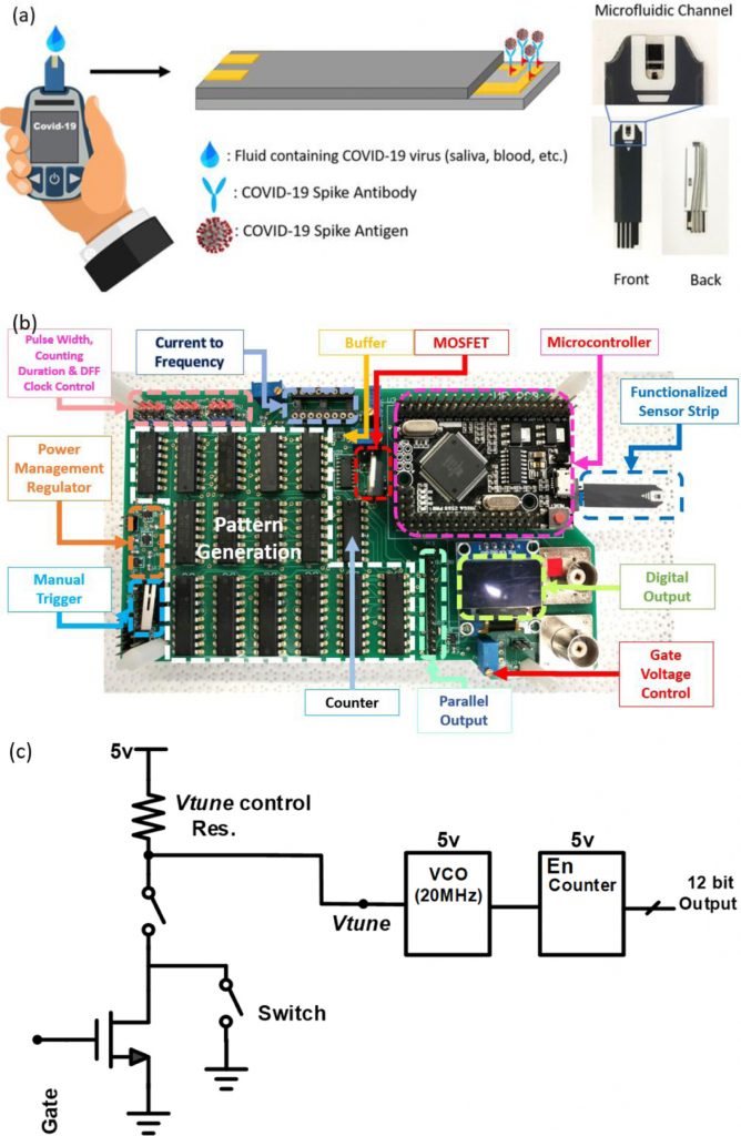 Figure Caption: Schematics and photograph of the sensor strip used in measurement (a), printed circuit board fabricated to produce digital sensor output with a built-in microcontroller (b) and architecture of a digital signal generation mechanism (c).
1098. “Review—Radiation Damage in Wide and Ultra-Wide Bandgap Semiconductors”, Minghan Xian, Hao Luo, Xinyi Xia, Chaker Fares, Patrick H. Carey, Chan-Wen Chiu, Fan Ren, Siang-Sin Shan, Yu-Te Liao, Shu-Min Hsu, Josephine F. Esquivel-Upshaw, Chin-Wei Chang, Jenshan Lin, Steven C. Ghivizzani, and 1041. Stephen J. Pearton, J. Vac. Sci. Technol. B39, 033202-7(2021).
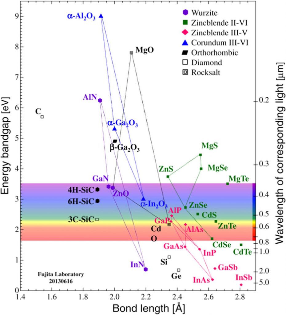 Figure Caption: Relationship between energy bandgap and bond length for various compound semiconductors promising for practical applications (adapted from Fujita, Japanese Journal of Applied Physics, 54, 030101 (2015), copyright IOP. All of the wide bandgap and ultra-wide bandgap materials of interest here can be grown in bulk form.
1097. “Design of Ga2O3 Modulation Doped Field Effect Transistors”, M.A. Mastro, M.J. Tadjer, J. Kim, F. Ren and S. J. Pearton, J.Vac. Sci. Technol. A 39, 023412 (2021).
1096. “Vertical beta-Ga2O3 Schottky rectifiers with 750V reverse breakdown voltage at 600K”, Xia, Xinyi; Xian, Minghan; Carey, Patrick; Fares, Chaker; Ren, Fan; Tadjer, Marko; Pearton, Stephen; Tu, Thieu Quang; Goto, Ken; Kuramata, Akito, J. Physics D: Appl. Phys. 54, 305103-8(2021).
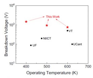 Figure Caption: Comparison of operation temperature versus maximum reverse bias for reported vertical Ga2O3 rectifiers. Previous data comes from Virginia Tech, University of Canterbury, University of Florida and NIICT.
1095. “Experimental estimation of electron–hole pair creation energy in beta-Ga2O3”, E. B. Yakimov, A. Y. Polyakov, I. V. Shchemerov, N. B. Smirnov, A. A. Vasilev, P. S. Vergeles,E. E. Yakimov, A. V. Chernykh, F. Ren, and S. J. Pearton, Appl. Phys. Lett., 118, 202106-5(2021).
1094. “Novel Coatings to Minimize Corrosion of Titanium in Oral Biofilm”, Samira Esteves Afonso Camargo, Tanaya Roy, Xinyi Xia, Chaker Fares, Shu-Min Hsu, Fan Ren, Arthur E. Clark, Dan Neal and Josephine F. Esquivel-Upshaw, Materials, 14, 342-10(2021).
1093. “Effect of probe geometry during measurement of >100 A Ga2O3 vertical rectifiers”, Ribhu Sharma, Minghan Xian, Chaker Fares, Mark E. Law, Marko Tadjer, Karl D. Hobart, Fan Ren, and Stephen J. Pearton, J. Vac. Sci. & Technol. A 39, 013406-10 (2021).
Experimental estimation of electron–hole pair creation energy in beta-Ga2O3
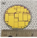 Figure Caption: Optical images of fabricated rectifiers on-wafer, showing a range of areas from 0.035 to 1.89 cm2.
2020
1092. “A Two electrode, Double Pulsed Sensor Readout Circuit for Cardiac Troponin I Measurement”, Siang Sin Shan, Shao Yung Lu, Yuan Po Yang, Su Ping Lin, Patrick Carey, M. Xian, FanRen, S.J. Pearton, Chin Wei Chang, J. Lin and Yu Te Liao, IEEE Trans Biomedical Circuits and Systems, 14, 1362 (2020).
 Figure Caption: Screening effects under different concentrations
 Figure Caption: Measurement setup
1091. “Photosensitivity of Ga2O3 Schottky diodes: Effects of deep acceptor traps present before and after neutron irradiation”, Z. Islam, M. Xian, A. Haque, F. Ren, M. Tadjer and S.J. Pearton, IEEE Trans. Electron Dev.67, 3056 (2020).
1090. “Band offset determination for amorphous Al2O3 deposited on bulk AlN and atomic-layer epitaxial AlN on sapphire”, Chaker Fares, Fan Ren,Marko J. Tadjer, Jeffrey Woodward, Michael A. Mastro, Boris N.Feigelson, Charles R. Eddy, Jr., and S. J.Pearton, Appl. Phys. Lett. 117, 182103-6 (2020).
Figure Caption: Band diagrams for (a) ALD Al2O3 on bulk AlN and (b) ALE AlN on a-plane sapphire (a-Al2O3).
1089. “Effect of probe geometry during measurement of >100 A Ga2O3 vertical rectifiers”, Ribhu Sharma, Minghan Xian, Chaker Fares, Mark E. Law, Marko Tadjer, Karl D. Hobart, Fan Ren, and Stephen J. Pearton, J. Vac. Sci. Technol. A39, 013406-10(2020).
1088. “Hydroxyapatite Formation on Coated Titanium Implants Submerged in Simulated Body Fluid”, Tatiana Aviles, Shu-Min Hsu , Arthur Clark, Fan Ren , Chaker Fares, Patrick H. Carey IV and Josephine F. Esquivel-Upshaw, Materials, 13, 5593-5617(2020).
Figure Caption: SEM of HA Formation Comparison (10 mscale). Scanning electron microscopy images taken at a field view of 50.0 µm with a 10 µm scale for (A) control; (B) sodium hydroxide; (C) quaternized titanium nitride; (D) silicon dioxide.
1087. “Titanium Corrosion in Peri-Implantitis”, Mailis D. Soler, Shu-Min Hsu , Chaker Fares, Fan Ren, Renita J. Jenkins, Luiz Gonzaga, Arthur E. Clark, Edgar O’Neil Dan Neal and Josephine F. Esquivel-Upshaw, Materials, 13, 5488-11(2020).
Figure Caption: (A) Radiographic image of Astra EV implant; (B) biopsy sample with possible metal particles identified (yellow arrows); (C) possible metal particle identified (red arrows) in resin-embedded biopsy sample under optical microscope
1086. “Design and implementation of floating field ring edge termination on vertical geometry beta-Ga2O3 Rectifiers”, Ribhu Sharma, Minghan Xian, Mark E. Law, Marko Tadjer, Fan Ren, and Stephen J. Pearton, J. Vac. Sci. Technol. A 38, 063414-9 (2020).
Figure Caption: Optical image of fabricated rectifier showing three field rings.
Figure Caption: (a) Simulated breakdown voltage and (b) percentage increase in breakdown voltage as a function of individual optimized parameters..
1085. “Novel methodology for measuring intraoral wear in enamel and dental restorative materials”, Josephine F. Esquivel-Upshaw, Shu-Min Hsu, Ana C. Bohórquez, Nader Abdulhameed, Gary W. Scheiffele, Mijin Kim, Dan Neal, John Chai and Fan Ren, Clin. Exp. Dent. Res., 1-9 (2020).
Figure Caption: (a) Representative zirconia crown on mandibular left first molar, second molar was used as a control alongside scans using Geomagic® Control X™ software (3D Systems, Rock Hill, SC) where baseline scans are superimposed with either 6 months or 1-year scans; (b) Opposing quadrant where maxillary first molar was used as the opposing enamel and the second molar was a control alongside intraoral scans. Scale indicate degrees of difference in microns between the two scans.
1084. “The Galvanic Effect of Titanium and Amalgam in the Oral Environment”, Patrick H. Carey IV, Shu-Min Hsu, Chaker Fares, George Kamenov, Fan Ren and Josephine Esquivel-Upshaw, Materials, 13, 4425-16 (2020).
Figure Caption: Optical images of Ti rods immersed in pH 2, pH 7, and pH 10 solution.
1083. “Role of hole trapping by deep acceptors in electron-beam-induced current measurements in beta-Ga2O3 vertical rectifiers”, E B Yakimov, A Y Polyakov, N B Smirnov, I V Shchemerov, P S Vergeles, E E Yakimov, A V Chernykh, Minghan Xian, F Ren and S J Pearton, J. Phys. D53, 495108-16 (2020).
1082. “Effect of pH Cycling Frequency on Glass–Ceramic Corrosion”, Shu-Min Hsu, Fan Ren, Christopher D. Batich, Arthur E. Clark, Dan Neal and Josephine F. Esquivel-Upshaw, Materials, 13, 3655-12 (2020).
Figure Caption: The SEM images of (a) reference (baseline) and corroded disks for 30 days of immersion in constant (b) pH 10, (c) pH 2, and (d) pH 7 and (e) 3-d cycling and (f) 1-d cycling.
1081. “In Situ Transmission Electron Microscopy Observations of Forward Bias Degradation of Vertical Geometry beta-Ga2O3 Rectifiers”, Zahabul Islam, Aman Haque, Nicholas Glavin, Minghan Xian, Fan Ren, Alexander Y. Polyakov, Anastasia Kochkova, Marko Tadjer, and S. J. Pearton, ECS J. Solid State Sci. Technol. 9, 055008-10(2020).
Figure Caption: (a) I-V characteristics under forward biasing condition; TEM bright field images at different biasing voltages: (b) 0 V, (c) 2.25 V, (d) 2.45 V, (e) 2.61 V, (f) 4.35 V, and (g) 4.81 V.
1080. “Impact of electron injection on carrier transport and recombination in unintentionally doped GaN”, Sushrut Modak, Leonid Chernyak, Minghan Xian, Fan Ren, Stephen J. Pearton, Sergey Khodorov, Igor Lubomirsky, Arie Ruzin, and Zinovi Dashevsky, J. Appl. Phys., 128, 085702-6(2020).
1079. “In Situ Observation of beta-Ga2O3 Schottky Diode Failure Under Forward Biasing Condition”, Zahabul Islam, Minghan Xian, Aman Haque , Fan Ren, Marko Tadjer , Nicholas Glavin, and Stephen Pearton, IEEE Trans. Electron Dev., 67, 3056-3061(2020).
Figure Caption: (a) SEM micrograph of bulk Ga2O3 SBD. (b) Coupon preparation from the bulk SBD device. (c) TEM cross section of the thin film SBD before mounting on the MEMS device. (d) MEMS chip on a TEM holder for in situ biasing. (e) Electron transparent sample mounted on the MEMS device. (f) Low magnification TEM BF image of beta-Ga2O3 SBD
1078. “Demonstration of a SiC Protective Coating for Titanium Implants”, Chaker Fares, Shu-Min Hsu, Minghan Xian, Xinyi Xia, Fan Ren, John J. Mecholsky, Jr., Luiz Gonzaga and Josephine Esquivel-Upshaw, Materials, 13, 3321-13 (2020).
Figure Caption: Scanning electron microscope images of a SiC-coated titanium implant at variousmagnifications. Image (a) shows the overall surface of the implant, whereas images (b–d) showdetailed images of the implant surface morphology at increasing magnifications
1077. “AlGaN/GaN heterostructure based Pt nanonetwork Schottky diode with water-blocking layer”, Kwang Hyeon Baik, Sunwoo Jung, Chu-Young Cho, Kyung-Ho Park, Fan Ren, Stephen. J. Pearton, Soohwan Jang, Sensor & Actuators B217, 128234-7(2020).
1076. “Dissolution activation energy of a fluorapatite glass-ceramic veneer for dental applications”, S.M. Hsu, F. Ren, C. Batich, A.E. Clark, V. Craciune, J.F. Esquivel-Upshaw, Mat/ Sci. & Eng. C111, 110802-7(2020).
1075. “Effect of Electron Injection on Minority Carrier Transport in 10 MeV Proton Irradiated beta-Ga2O3 Schottky Rectifiers”, Sushrut Modak, Leonid Chernyak, Sergey Khodorov, Igor Lubomirsky, Arie Ruzin, Minghan Xian, Fan Ren and Stephen J. Pearton, ECS JSST 9, 045018-5(2020).
1074. “Novel Coating to Minimize Corrosion of Galss-Ceramics for Dental applications”, Shu-Min Hsu, Fan Ren, Zhiting Chen, Mijin Lim, Arthur E. Clark, Dan Neal and Josephine F Esquivel-Upshaw, Materials, 13, 1215-1226(2020).
1073. “Anti-Bacterial Properties and Biocompatibility of Novel SiC Coating for Dental Ceramic”, Samira Esteves Afonso Camargo, Azeem S. Mohiuddeen, Chaker Fares, Jessica Partain, Patrick H. Carey IV, Fan Ren, Shu-Min Hsu, Arthur E. Clark, and Josephine F Esquivel-Upshaw, J. Functional Biomat., 11 33-46(2020).
1072. “Annealing & N2 Plasma Treatment to Minimize Corrosion of SiC Coated Glass-Ceramics”, Chaker Fares, Randy Elhassani, Jessica Partain, Shu-Min Hsu, Valentin Craciun, Fan Ren, and Josephine F Esquivel-Upshaw, Materials, 13, 2375-2388(2020).
1071. “High Temperature Operation to 500°C of AlGaN Graded Polarization Doped Field Effect Transistors”, Patrick H. Carey IV, Fan Ren, Andrew M. Armstrong, Brianna A. Klein, Andrew A. Allerman, Erica A. Douglas, Albert G. Baca, Stephen J. Pearton, J. Vac. Sci. Technol. B 38, 033202 (2020).
Figure Caption: (a) Device schematic and epitaxial structure of the POLFET and (b) BF-TEM image of epitaxial structure with gate contact.
1070. “Annealing Effects on the Band Alignment of ALD SiO2 on (InxGa1-x)2O3 for x = 0.25–0.74”, Chaker Fares, Minghan Xian, David J. Smith, M. R. McCartney, Max Kneiß, Holger von Wenckstern, Marius Grundmann, Marko Tadjer, Fan Ren, and S. J. Pearton, ECS J. Solid State Sci. Technol., 9, 045001 (2020).
Figure Caption: High-resolution TEM images and corresponding fast Fourier transforms (FFT) from (a)–(b) the bottom of the gallium-rich portion and (c)–(d) the bottom of the indium-rich portion of the (InxGa1-x)2O3 wafer
1068. “Alpha Particle Irradiation of High Aluminum Content AlGaN Polarization Doped Field Effect Transistors”, Patrick H. Carey IV, Fan Ren, Jinho Bae, Jihyun Kim, and Stephen J. Pearton, ECS J. Solid State Sci. Technol.9, 035008-6(2020).
1068. “Changes in Band Alignment During Annealing at 600°C of ALD Al2O3 on (InxGa1-x)2O3 for x= 0.25 to 0.74 ”, Chaker Fares, Minghan Xian, David J. Smith, Martha R. McCartney, Max Kneiß, Holger von Wenckstern, Marius Grundmann, Marko Tadjer, Fan Ren and S.J. Pearton, J. Appl. Phys. 127, 105701 (2020).
1067. “Asymmetrical Contact Geometry to Reduce Forward Bias Degradation in beta Ga2O3 Rectifiers”, Minghan Xian, Chaker Fares, Fan Ren, Zahabul Islam, Aman Haque, Marko Tadjer and S. J. Pearton, ECS J. Solid State Sci. Technol.9, 035007(2020).
1066. “Novel Coating to Minimize Corrosion of Glass-Ceramics for Dental Applications”, Shu-Min Hsu, Fan Ren, Zhiting Chen, Mijin Kim, Chaker Fares, Arthur E Clark, Dan Neal and Josephine F Esquivel-Upshaw, Materials 13, 1215(2020).
1065. “Proton Irradiation of High Aluminum Content AlGaN Polarization Doped Field Effect Transistors”, Patrick H. CareyIV, Fan Ren, Jinho Bae, Jihyun Kim, and Stephen J. Pearton, ECS J. Solid State Sci. Technol., 9, 025003-6 (2020).
1064. “Plasma etching of wide bandgap and ultrawide bandgap semiconductors”, Stephen J. Pearton, Erica A. Douglas, Randy J. Shul, and Fan Ren, J. Vac. Sci. & Technol. A 38, 020802-15(2020).
1063. “Review—Opportunities for Rapid, Sensitive Detection of Troponin and Cerebral Spinal Fluid Using Semiconductor Sensors”, Patrick H. Carey IV, Brian C. Lobo, Michael P. Gebhard, Marino E. Leon, Sherri D. Flax, Neil S. Harris, Yu-Te Liao, Chin-Wei Chang, Jenshan Lin, Fan Ren, and S. J. earton, J. Electrochem. Soc., 167 037507-8(2020).
Figure Caption: Photograph of a prototype design, including readouts, microcontroller, signal processing units, and display. BNC connectors are used for the current design, and they will be replaced with strip clip connectors once the configuration of the sensor chip is optimized.
2019
1062. “Annealing of Proton and Alpha Particle Damage in Au-W/beta-Ga2O3 Rectifiers”, Minghan Xian, Chaker Fares, Jinho Bae, Jihyun Kim, Fan Ren, and S. J. Pearton, J. Solid State Sci. Technol., 8 (12) P799-P804 (2019).
Figure Caption: Schematic of conventional (left) and thinned-down (right) rectifier structures.
1061. “Optimization of Edge Termination Techniques for beta-Ga2O3 Schottky Rectifiers”, Ribhu Sharma, Erin E. Patrick, M. E. Law, F. Ren, and S. J. Pearton, ECS J. Solid State Sci. Technol., 8 (12) Q234-Q239 (2019).
Figure Caption: (a) Structure of the simulated Schottky diode based on literature. (b) Field-plated diode structure with 2 variables, i.e. Field plate overlap (OL) and dielectric thickness (t). (c) Fieldplated diode pillar dielectric structure with a variable pillar height (HP). (d) Field-plated diode step dielectric structure with variable step height (HS). (e–g) Various structures simulated with Argon ion implanted resistive regions. The optimized solution between the ion implanted structures (e–g) according to the simulations would be (e) i.e. a highly resistive infinite implanted region.
1060. “Effect of Annealing on the Band Alignment of ALD SiO2 on (AlxGa1-x)2O3 for x = 0.2 – 0.65”, Chaker Fares, Zahabul Islam, Aman Haque, Max Kneiß, Holger von Wenckstern, Marius Grundmann, Marko Tadjer, Fan Ren, and S. J. Pearton, ECS J. Solid State Sci. Technol., 8 (12) P751-P756 (2019).
Figure Caption: Bright Field (BF) TEM images and selected area diffraction pattern (SAED) from (Al0.20Ga0.80)2O3: (a) low magnification BF image, (b) High magnification BF images, (c) atomic resolution BF image, and (d) SAED image.
1059. “Extreme Temperature Operation of Ultra-Wide Bandgap AlGaN High Electron Mobility Transistors”, Patrick H. Carey, IV, Fan Ren, Albert G. Baca, Brianna A. Klein, Andrew A. Allerman, Andrew M. Armstrong, Erica A. Douglas, Robert J. Kaplar, Paul G. Kotula, and Stephen J. Pearton, Trans Semicond. Manufacu., 21, 473-437(2019).
Figure Caption: Comparison of 4H-SiC, GaN, beta-Ga2O3, and Al0.7Ga0.3N critical electric field, thermal conductivity, electron mobility, saturation velocity and energy bandgap.
1058. “Opportunities and Challenges in MOCVD of beta-Ga2O3 for Power Electronic Devices”, M. A. Mastro, J. K. Hite, C. R. Eddy, Jr., and M. J. Tadjer, S. J. Pearton, F. Ren, and J. Kim, Intern. J. High Speed Electronics & Systems, 28, 1940007-18(2019).
Figure Caption: Properties of relevant semiconductor materials and normalized unipolar power-device figures of merit (FOM).
1057. “Forward bias degradation and thermal simulations of vertical geometry beta-Ga2O3 Schottky rectifiers”, Minghan Xian, Randy Elhassani, Chaker Fares, Fan Ren, Marko Tadjer, and S. J. Pearton, J. Vac. Sci. & Technol. B37, 061205-6 (2019).
1056. “Effects of Hydrogen Plasma Treatment Condition on Electrical Properties of beta-Ga2O3”, A. Y. Polyakov, In-Hwan Lee, N. B. Smirnov, E. B. Yakimov, I. V. Shchemerov, A. V. Chernykh, A. I. Kochkova, A. A. Vasilev, A. S. Shiko,1 Patrick H. Carey IV, F. Ren, and S. J. Pearton, ECS J. Solid State Sci. Technol.8, P661-P666(2019).
Figure Caption: (a) Deuterium concentration profiles measured at two temperatures for treatments under harsh plasma conditions; (b) Deuterium concentration profiles after treatment at 200°C under harsh plasma conditions and annealed in nitrogen at 400°C and 500°C.
1055. Effect of thermal annealing for W/beta-Ga2O3 Schottky diodes up to 600°C”, Minghan Xian, Chaker Fares, Fan Ren, Brent P. Gila, Yen-Ting Chen, Yu-Te Liao, Marko Tadjer, and Stephen J. Pearton, J. Vac. Sci. & Technol. B37, 061201-6 (2019).
1054. “Valence band offsets for ALD SiO2 and Al2O3 on (InxGa1-x)2O3 for x = 0.25–0.74”, Chaker Fares, Max Kneiß, Holger von Wenckstern , Marius Grundmann , Marko Tadjer, Fan Ren, Eric Lambers, and S. J. Pearton, APL Mater. 7, 071115 (2019).
1053. “Implementation of a 900 V switching circuit for high breakdown voltage beta-Ga2O3 Schottky diodes”, Yen Ting Chen, Jiancheng Yang, Fan Ren, Chin Wei Chang, Jenshan Lin, S. J. Pearton, Marko J Tadjer, and Akito Kuramata and Yu Te Liao, ECS J. Solid State Sci. Technol.8, Q3231 (2019).
1052. “Diffusion of implanted Ge and Sn in beta-Ga2O3”, Ribhu Sharma, Mark E. Law, Minghan Xian, Marko Tadjer, Elaf A. Anber, Daniel Foley, Andrew C. Lang, James L. Hart, James Nathaniel, Mitra L. Taheri, Fan Ren, S. J. Pearton, and A. Kuramata, J. Vac. Sci. & Technol. B37, 051204-5 (2019).
1051. “Hydrogen plasma treatment of beta-Ga2O3: Changes in electrical properties and deep trap spectra”, A. Y. Polyakov, In-Hwan Lee, N. B. Smirnov, E. B. Yakimov, I. V. Shchemerov, A. V. Chernykh, A. I. Kochkova, A. A. Vasilev, F. Ren, P. H. Carey IV, and S. J. Pearton, Apply, Phys, Lett., 115 (2019).
1050. “Fast Cerebrospinal Fluid Detection Using Inexpensive Modular Packaging with Disposable Testing Strips”, Patrick H. Carey IV, Jiancheng Yang, Fan Ren, Yu-Te Liao, Chin-Wei Chang, Jenshan Lin, Stephen J. Pearton, Brian Lobo and Marino E. Leon, J. ECS, 166 B708-B712(2019).
1049. “Defects at the surface of beta-Ga2O3 produced by Ar plasma exposure”, Patrick H. Carey IV, Fan Ren, Ziqi Jia, Christopher D Batich, Samira E. A. Camargo, Arthur E. Clark, Valentin Craciun, Daniel W. Neal, and Josephine F. Esquivel-Upshaw, Chem. Select, 4, 9185 –9189 (2019).
Figure Caption: Summary of energy levels and their concentration detected before and after Ar plasma exposure. The length of the bars represents the relative concentrations.
1048. “Demonstration of SiO2/SiC-based protective coating for dental ceramic prostheses”, Zhiting Chen, Chaker Fares, Randy Elhassani, Fan Ren, Mijin Kim, Shu-Min Hsu, Arthur E. Clark and Josephine F. Esquivel-Upshaw, J. American Ceramic Soc., 102, 6591-6599(2019).
Figure Caption: Substrate, SiC thickness, and corresponding detalE of each coated disk that was matched to the Vita shade Guide. A constant thickness of 20 nm SiO2 was utilized prior to SiC deposition.
1047. “Antibacterial Properties of Charged TiN Surfaces for Dental Implant Application”, Patrick H. Carey IV, Fan Ren, Ziqi Jia, Christopher D Batich, Samira E. A. Camargo, Arthur E. Clark, Valentin Craciun, Daniel W. Neal, and Josephine F. Esquivel-Upshaw, Chem. Select, 4, 9185 –9189 (2019).
Figure Caption: Fluorescence microscopy images of S. mutans cultured for 4 h on Ti, TiN or quaternized TiN substrate.
1046. “Valence band offsets for ALD SiO22 and Al2O3 on (AlxGa1-x)2O3 for x = 0.25-0.7”, Chaker Fares, Max Knei, Holger von Wenckstern, Marko Tadjer, Fan Ren, Eric Lambers, Marius Grundmann, and S. J. Pearton, APL Mater. 7, 071115(2019).
Figure Caption: Band diagrams for the Al2O3/(InxGa1-x)2O3 heterostructure in which the Al2O3 was deposited by ALD.
1045. “Will surface effects dominate in quasi-two dimensional gallium oxide for electronic and photonic devices?”, Jihyun Kim, F. Ren and S. J. Pearton, Royal Soc. Chemistry, Nanoscale Horizons, 4, 1251(2019).
1044. “Band Alignment of Atomic Layer Deposited SiO2 and Al2O3 on (AlxGa1-x)2O3 for x = 0.2-0.65”, Chaker Fares, Max Knei, Holger von Wenckstern, Marko Tadjer, Fan Ren, Eric Lambers, Marius Grundmann, and S. J. Pearton, ECS J. Solid State Sci. Technol.8, P351-P356(2019).
1043. “Vertical geometry 33.2 A, 4.8 MW/cm2 Ga2O3 field-plated Schottky rectifier arrays”, Jiancheng Yang, Minghan Xian,1 Patrick Carey, Chaker Fares, Jessica Partain, Fan Ren, Marko Tadjer, Elaf Anber, Dan Foley, Andrew Lang, James Hart, James Nathaniel, Mitra L. Taheri, S. J. Pearton, and Akito Kuramata, Appl. Phys. Lett. 114, 232106 (2019).
1042. “Impact of Electron Injection and Temperature on Minority Carrier Transport in Alpha Irradiated beta-Ga2O3 Schottky Rectifiers”, Sushrut Modak, Leonid Chernyak, Sergey Khodorov, Igor Lubomirsky, Jiancheng Yang, Fan Ren and S. J. Pearton, ECS J. Solid State Sci. Technol. 8, Q3050 (2019).
1041. “Thermal Simulations of High Current beta-Ga2O3 Schottky Rectifiers”, PRohit Sharma, Erin Patrick, Mark E. Law, Jiancheng Yang, F. Ren and S.J. Pearton, ECS J. Solid State Sci. Technol.8, Q3195 (2019).
1040. “Comparison of Dual-Stack Dielectric Field Plates on beta-Ga2O3 Schottky Rectifiers”, Patrick H Carey IV, Jiancheng Yang, Fan Ren, Ribhu Sharma, Mark Law, and Stephen J. Pearton, ECS J. Solid State Sci. & Technol., 8, Q3211-Q3225(2019).
1039. “Operation up to 500°C of Al0.85Ga0.15N/Al0.7Ga0.3N High Electron Mobility Transistors”, Patrick H. Carey, IV,Fan Ren, Albert G. Baca, Brianna A. Klein, Andrew A. Allerman, Andrew M. Armostrong, Erica A. Douglas, Robert J. Kaplar, Paul G. Kotula, and Stephen J. Pearton, J Electron Dev. Soc. 7, 444-453 (2019).
Figure Caption: IDS-VDS curves for AlGaN-channel devices from 25-500°C.
1038. “Valence and Conduction Band Offsets for InN and III-Nitride Ternary Alloys on (-201) Bulk beta-Ga2O3”, Chaker Fares, Marko J. Tadjer, Jeffrey Woodward, Neeraj Nepal, Michael A. Mastro, Charles R. Eddy Jr., Fan Ren, and Stephen J. Pearton, ECS J. Solid State Sci. & Technol., 8, Q3154-Q3158(2019).
1037. “Reverse Breakdown in Large Area, Field-Plated, Vertical beta-Ga2O3 Rectifiers”, Jiancheng Yang, Chaker Fares, Randy Elhassani, Minghan Xian, Fan Ren, S. J. Pearton, Marko Tadjer, and Akito Kuramata, ECS J. Solid State Sci. & Technol., 8, Q3159-Q3164(2019).
1036. “Comprehensive analysis of laserscanner validity used for measurement of wear”, Shu-Min Hsu, Fan Ren, Nader Abdulhameed, Mijin Kim, Dan Neal, Josephine Esquivel-Upshaw, J Oral Rehabil. 46, 503-510(2019).
1035. ” 2D Material-Based Vertical Double Heterojunction Bipolar Transistors with High Current Amplification”, Geonyeop Lee, Stephen J. Pearton, Fan Ren, and Jihyun Kim, Adv. Electron. Mater., 5, 1800745-1-7(2019).
1034. “Damage Recovery and Dopant Diffusion in Si and Sn Ion Implanted beta-Ga2O3“, Marko J. Tadjer, Chaker Fares, Nadeemullah A. Mahadik, Jaime A. Freitas Jr., David Smith, Ribhu Sharma, 4 Mark E. Law, Fan Ren, S. J. Pearton, and A. Kuramata, ECS JSST, 8, Q3133-Q3139 (2019).
1033. ” Deep traps and persistent photocapacitance in beta-(Al0.14Ga0.86)2O3/Ga2O3 heterojunctions”, A. Y. Polyakov, N. B. Smirnov, I. V. Schemerov, A. V. Chernykh, E. B. Yakimov, A. I. Kochkova, Jiancheng Yang, Chaker Fares, F. Ren, and S. J. Pearton, J. Appl. Phys. 125, 095702-11(2019).
1032. “Dynamic Switching Characteristics of 1 A Forward Current beta-Ga2O3 Rectifiers”, J. Yang, F. Ren, Y.-T. Chen, Y.-T. Liao, C.-W. Cang, J. S. Lin, M. J. Tadjer, S. J. Pearton and A. Kuramata, J. Electron Dev. Soc., 7, 57-62(2019).
1031. ” 60Co Gamma Ray Damage in Homoepitaxial beta-Ga2O3 Schottky Rectifiers”, J. Yang, G. J. Koller, Chaker Fares, F. Ren, S. J. Pearton, J. Bae, Jihyun Kim, and D. J. Smith, ECS JSST, 8, Q3041-Q3045 (2019).
1030. ” Valence- and Conduction-Band Offsets for Atomic-Layer-Deposited Al2O3 on (010) (Al0.14Ga0.86)2O3”, C. Fares, F. Ren, E. Lambers, D. C. Hays, B.P. Gila, and S.J. Pearton, J. Electronic Mat., 48, 1568-1572(2019).
1029. ” Valence and conduction band offsets for sputtered AZO and ITO on (010) (Al0.14Ga0.86)2O3”, Chaker Fares, F Ren, Eric Lambers, David C Hays, B P Gila, and S J Pearton, Semicond. Sci. Technol. 34, 025006 (2019).
1028. “Device processing and junction formation needs for ultra-high power Ga2O3 electronics”, F. Ren, J.C. Yang, C. Fares and S.J. Pearton, MRS Communications, 1-11 (2019).
1027. ” Switching Behavior and Forward Bias Degradation of 700V, 0.2A, beta-Ga2O3 Vertical Geometry Rectifiers”, J. Yang, C. Fares, F. Ren, Y.-T. Chen, Y.-T. Liao, C.-W. Chang, J. Lin, M. Tadjer, D. J. Smith, S. J. Pearton,and A. Kuramata, ECS J. Solid State Sci. and Technol., 8, Q3028-Q3033 (2019).
1026. “Radiation damage effects in Ga2O3 materials and devices”, Jihyun Kim, Stephen J. Pearton, Chaker Fares, Jiancheng Yang, Fan Ren, Suhyun Kima and Alexander Y. Polyakovd J. Mater. Chem., C7, 10-25 (2019).
2018
1025. “Perspective: Ga2O3 for ultra-high power rectifiers and MOSFETS”, S. J. Pearton, Fan Ren, Marko Tadjer, and Jihyun Kim, J. Applied Phys. 124, 220901 (2018).
1024. “Hydrogen Sensing Characteristics of Pt Schottky Diodes on (-201) and (010) Ga2O3 Single Crystals” Soohwan Jang, Sunwoo Jung, Jihyun Kim, Fan Ren, Stephen J. Pearton, and Kwang Hyeon Baik, ECS J. Solid State Sci. & and Technol. 7 (7) Q3180-Q3182 (2018).
1023. “Effect of 1.5 MeV electron irradiation on beta-Ga2O3 carrier lifetime and diffusion length” Jonathan Lee, Elena Flitsiyan, Leonid Chernyak, Jiancheng Yang, Fan Ren, Stephen J. Pearton, Boris Meyler, and Y. Joseph Salzman, Appl. Phys. Lett. 112, 082104-6 (2018).
1022. “Zika virus detection using antibody-immobilized disposable cover glass and AlGaN/GaN high electron mobility transistors” Jiancheng Yang, Patrick Carey, Fan Ren, Michael A. Mastro, Kimberly Beers, S. J. Pearton, and Ivan I. Kravchenko, Appl. Phys. Lett. 113, 032101-6 (2018).
1021. “Band Offsets for Atomic Layer Deposited HfSiO4 on (Al0.14Ga20.86)2O3” Chaker Fares, F. Ren, Eric Lambers, David C. Hays, B. P. Gila, and S. J. Pearton, ECS J. Solid State Sci. & and Technol. 7 (10) P519-P523 (2018).
1020. “Electrical properties of bulk semi-insulating beta-Ga2O3(Fe)” A. Y. Polyakov, N. B. Smirnov, I. V. Shchemerov, S. J. Pearton, Fan Ren, A. V. Chernykh, and A. I. Kochkova, Appl. Phys. Lett. 113, 142102-5 (2018).
1019. “Band alignment of atomic layer deposited SiO2 on (010) (Al0.14Ga20.86)2O3” Chaker Fares, F. Ren, Eric Lambers, David C. Hays, B. P. Gila, and S. J. Pearton, J. Vac. Sci. & Technol. B36, 061207-7 (2018).
1018. “Effect of alpha-particle irradiation dose on SiNx/AlGaN/GaN metal–insulator semiconductor high electron mobility transistors” Chaker Fares, Fan Ren, Stephen J. Pearton, Gwangseok Yang, Jihyun Kim, Chien-Fong Lo, and J. Wayne Johnson, J. Vac. Sci. & Technol. B36,, 041203-6 (2018).
1017. “Valence band offsets for CuI on (-201) bulk Ga2O3 and epitaxial (010) (Al0.14Ga0.86)2O3” Chaker Fares, F. Ren, David C. Hays, B. P. Gila, Marko Tadjer, Karl D. Hobart, and S. J. Pearton, Appl. Phys. Lett. 113, 182101-6 (2018).
1016. “Effect of surface treatments on electrical properties of beta-Ga2O3” Jiancheng Yang, Zachary Sparks, Fan Ren, Stephen J. Pearton, and Marko Tadjer, J. Vac. Sci. & Technol. B36, 061201-1-9 (2018).
1015. “Effect of proton irradiation energy on SiNx/AlGaN/GaN metal-insulator semiconductor high electron mobility transistors” Chaker Fares, Fan Ren, Stephen J. Pearton, Gwangseok Yang, Jihyun Kim, Chien-Fong Lo, and J. Wayne Johnson, J. Vac. Sci. & Technol. B36 052202-1-6 (2018).
1014. “Vertical Geometry, 2-A Forward Current Ga2O3 Schottky Rectifiers on Bulk Ga2O3 Substrates” Jiancheng Yang, Fan Ren, Steve J. Pearton, and Akito Kuramata, IEEE Trans on Electron Dev., 65, 2790-2796(2018).
1013. “Defects responsible for charge carrier removal and correlation with deep level introduction in irradiated beta-Ga2O3“ A. Y. Polyakov, N. B. Smirnov, I. V. Shchemerov, E. B. Yakimov, S. J. Pearton, Chaker Fares, Jiancheng Yang, Fan Ren, Jihyun Kim, P. B. Lagov,1,6 V. S. Stolbunov, and A. Kochkova, Appl. Phys. Lett., 113, 092102 (2018).
1012. “Ga2O3 Schottky rectifiers with 1 ampere forward current, 650 V reverse breakdown and 26.5 MW/cm2 figure-of-merit” Jiancheng Yang, F. Ren, Marko Tadjer, S. J. Pearton, and A. Kuramata, AIP Advances 8, 055026 (2018).
1011. “2300V Reverse Breakdown Voltage Ga2O3 Schottky Rectifiers” Jiancheng Yang, F. Ren, Marko Tadjer, S. J. Pearton, and A. Kuramata4, ECS J. Solid State Science & Technol., 7, Q92-Q96 (2018).
1010. “Diffusion length of non-equilibrium minority charge carriers in beta-Ga2O3 measured by electron beam induced current” E. B. Yakimov, A. Y. Polyakov, N. B. Smirnov, I. V. Shchemerov, Jiancheng Yang, F. Ren, Gwangseok Yang, Jihyun Kim, and S. J. Pearton, J. Appl. Phys., 123, 185704 (2018).
1009. “Eighteen mega-electron-volt alpha-particle damage in homoepitaxial beta-Ga2O3 Schottky Rectifiers” Jiancheng Yang, Chaker Fares, Yu Guan, F. Ren, S. J. Pearton, Jinho Bae, Jihyun Kim, and Akito Kuramata, J. Vac. Sci. & Technol. B36 031205-1-4 (2018).
1008. “Effects of fluorine incorporation into Beta-Ga2O3” Jiangcheng Yang, Chaker Fares, F. Ren, Ribhu Sharma, Erin Patrick, Mark E. Law, S. J. Pearton, and Akito Kuramata, J. Appl. Phy., 123, 165706 (2018).
1007. “AlGaN/GaN Heterostructure Based Schottky Diode Sensors with ZnO Nanorods for Environmental Ammonia Monitoring Applications” Sunwoo Jung, Kwang Hyeon Baik, Fan Ren, S. J. Pearton, and Soohwan Jang, ECS J. Solid State Sci. & Technol. 7(7) Q3020-Q3024(2018).
1006. “Moisture Insensitive PMMA Coated Pt-AlGaN/GaN Diode Hydrogen Sensor and Its Thermal Stability” Kwang Hyeon Baik, Sunwoo Jung, Fan Ren, S. J. Pearton, and Soohwan Jang, ECS J. Solid State Sci. & Technol. 7(7) Q3009-Q3013(2018).
1005. “10 MeV proton damage in beta-Ga2O3 Schottky rectifiers” iancheng Yang, Zhiting Chen, Fan Ren, S. J. Pearton, Gwangseok Yang, Jihyun Kim, Jonathan Lee, Elena, Flitsiyan, Leonid Chernyak, and Akito Kuramata, J. Vac. Sci. & Technol. B36 011206-1-4 (2018).
1004. “Point defect induced degradation of electrical properties of Ga2O3 by 10 MeV proton Damage” A. Y. Polyakov, N. B. Smirnov, I. V. Shchemerov, E. B. Yakimov, Jiancheng Yang, F. Ren, Gwangseok Yang, Jihyun Kim, A. Kuramata, and S. J. Pearton, Appl. Phys. Lett., 112, 032107-1-1(2018).
1003. “Randomized clinical study of wear of enamel antagonists against polished monolithic zirconia crowns” J.F. Esquivel-Upshawa, M.J. Kim, S.M. Hsu, N. Abdulhameed R. Jenkins, D. Neal, F. Ren, A.E. Clarka, J. Dentistry 68, 19–27(2018).
1002. “Novel Testing for Corrosion of Glass-Ceramics for Dental Applications” J.F. Esquivel-Upshaw, F. Ren, S.M. Hsu, F.Y. Dieng, D. Neal, and A.E. Clark, J. of Dental Research, 97(3), 296-302 (2018).
1001. “A review of Ga2O3 materials, processing, and devices” S. J. Pearton, Jiancheng Yang, Patrick H. Cary, F. Ren, Jihyun Kim, Marko J. Tadjer, and Michael A. Mastro, Appl. Phys. Rev., 5, 011301-1-57 (2018).
1000. “Trapping Phenomena in InAlN/GaN High Electron Mobility Transistors” A. Y. Polyakov, N. B. Smirnov, I. V. Shchemerov, Jiancheng Yang, Fan Ren, Chien-Fong Lo, Oleg Laboutin, J. W. Johnson, and S. J. Pearton, ECS J. Solid State Sci. & Technol., 7 (2) Q1-Q7 (2018).
999. “A comparative study of wet etching and contacts on (201) and (010) oriented beta-Ga2O3” Soohwan Jang, Sunwoo Jung, Kimberly Beers, Jiancheng Yang, Fan Ren, A. Kuramata, S.J. Pearton, Kwang Hyeon Baik, J. Alloys and Compounds, 731, 118-125(2018).
2017
998. “Temperature and Humidity Dependence of Response of PMGI-Encapsulated Pt-AlGaN/GaN Diodes for Hydrogen Sensing” Sunwoo Jung, Kwang Hyeon Baik, Fan Ren, Stephen J. Pearton, and Soohwan Jang, IEEE Sensors J., 17, 5817-5822(2017).
997. “Annealing of dry etch damage in metallized and bare (-201) Ga2O3” Jiancheng Yang, Fan Ren, Rohit Khanna, Kristen Bevlin, Dwarakanath Geerpuram, Li-Chun Tung, Jingyu Lin, Hongxing Jiang, Jonathan Lee, Elena Flitsiyan, Leonid Chernyak, S. J. Pearton, and Akito Kuramata, J. Vac. Sci. & Technol., B35, 051201-1-6(2017).
996. “Ohmic contacts on n-type beta-Ga2O3 using AZO/Ti/Au” Patrick H. Carey IV, Jiancheng Yang, F. Ren, David C. Hays, S. J. Pearton, Soohwan Jang, Akito Kuramata, and Ivan I. Kravchenko, AIP Advances, 7, 095313-1-7(2017).
995. “Rapid detection of cardiac troponin I using antibody-immobilized gate-pulsed AlGaN/GaN high electron mobility transistor structures” Jiancheng Yang, Patrick Carey, Fan Ren, Yu-Lin Wang, Michael L. Good, Soohwan Jang, Michael A. Mastro, and S. J. Pearton, Appl. Phys. Lett., 111 202104(2017).
994. “Influence of High-Energy Proton Irradiation on beta-Ga2O3 Nanobelt Field-Effect Transistors” Gwangseok Yang, Soohwan Jang, Fan Ren, Stephen J. Pearton, and Jihyun Kim, ACS Applied Materials & Interfaces, 9, 40471-40476(2017).
993. “Silver-Functionalized AlGaN/GaN Heterostructure Diode for Ethanol Sensing” Sunwoo Jung, Kwang Hyeon Baik, Fan Ren, S. J. Pearton, and Soohwan Jang, J. Electrochem. Soc., 164, B417-B420 (2017).
992. “Band alignment of atomic layer deposited SiO2 and HfSiO4 with (-201) beta-Ga2O3” Patrick H. Carey, Fan Ren, David C. Hays, Brent P. Gila, Stephen J. Pearton, Soohwan Jang, and Akito Kuramata, Japanese J. of Appl. Phys., 56, 071101 (2017).
991. “Detection of ammonia at low concentrations (0.1–2 ppm) with ZnO nanorod-functionalized AlGaN/GaN high electron mobility transistors” Sunwoo Jung, Kwang Hyeon Baik, Fan Ren, Stephen J. Pearton, Soohwan Jang, J. Vac. Sci. Technol. B35, 042201-1-5(2017).
990. “High Breakdown Voltage (-201) beta-Ga2O3 Schottky Rectifiers” Jiancheng Yang, Shihyun Ahn, F. Ren, S. J. Pearton, Soohwan Jang, and A. Kuramata, IEEE Electron Dev. Lett., 38, 906-909(2017).
989. “Band offsets in ITO/Ga2O3 heterostructures” Patrick H. Carey IV, F. Ren, David C. Hays, B.P Gila, S.J. Pearton, Soohwan Jang, Akito Kuramata, Applied Surface Science 422, 179–183(2017).
988. “Conduction and valence band offsets of LaAl2O3 with (201) beta-Ga2O3” Patrick H. Carey IV, Fan Ren, David C. Hays, Brent P. Gila, and Stephen J. Pearton, Soohwan Jang and Akito Kuramata, J. Vac. Sci. Technol. B35, 041201-5(2017).
987. “1.5MeV electron irradiation damage in beta-Ga2O3 vertical rectifiers” Jiancheng Yang, Fan Ren, Stephen J. Pearton, Gwangseok Yang, Jihyun Kim and Akito Kuramata, J. Vac. Sci. Technol., 35B, 031208-5 (2017).
986. “Band alignment of Al2O3 with (-201) beta-Ga2O3” Patrick H. Carey IV, F. Ren, David C. Hays, B.P. Gila, S.J. Pearton, Soohwan Jang, Akito Kuramata, Vacuum, 142, 52-57 (2017).
985. “High reverse breakdown voltage Schottky rectifiers without edge termination on Ga2O3” Jiancheng Yang, Shihyun Ahn, F. Ren, S. J. Pearton, Soohwan Jang, Jihyun Kim, and A. Kuramata, Appl. Phys. Lett., 110, 182101-5 (2017).
984. “Pt-AlGaN/GaN hydrogen Sensor with water-blocking PMMA layer” Sunwoo Jung, Kwang Hyeon Baik, Fan Ren, Stephen J. Pearton, and Soohwan Jang, IEEE Electron Dev. Lett., 38, 657-660 (2017).
983. “Valence and conduction band offsets in AZO/Ga2O3 heterostructures” Patrick H. Carey IV, F. Ren, David C. Hays, B.P. Gila, S.J. Pearton, Soohwan Jang, Akito Kuramata, Vacuum, 141, 103-108 (2017).
982. “Inductively coupled plasma etch damage in (-201) Ga2O3 Schottky diodes” Jiancheng Yang, Shihyun Ahn, F. Ren, Rohit Khanna, Kristen Bevlin, Dwarakanath Geerpuram, S. J. Pearton, and A. Kuramata, Appl. Phys. Lett., 110, 142101-5(2017).
981. “Inductively coupled plasma etching of bulk, single-crystal Ga2O3” Jiancheng Yang, Shihyun Ahn, and Fan RenStephen PeartonRohit Khanna, Kristen Bevlin, and Dwarakanath Geerpuram, Akito Kuramata, J. Vac. Sci. Technol. B35, 031205-8(2017).
980. “Energy band offsets of dielectrics on InGaZnO4”, David C. Hays, B. P. Gila, S. J. Pearton, and F. Ren, Appl. Phys. Rev., 4, 021301-22 (2017).
979. “Opportunities and Future Directions for Ga2O3” Michael A. Mastro, Akito Kuramata, Jacob Calkins, Jihyun Kim, Fan Ren and S. J. Pearton, ECS J. Solid State Sci, & Technol., 6, P356-p359 (2017).
978. “Tuning the thickness of exfoliated quasi-two-dimensional beta-Ga2O3 flakes by plasma etching” Rudawski, M.R. Holzworth, S.J. Pearton, K.S. Jones, L. Liu, T.S. Kang, F. Ren, Microelectron. Rel., 70, 41-48 (2017).
977. “Erosion defect formation in Ni-gate AlGaN/GaN high electron mobility transistors”, P.G. Whiting, M.R. Holzworth, A.G. Lind, S.J. Pearton, K.S. Jones, L. Liu, T.S. Kang, F. Ren, Y. Xin, Microelectron Rel. 70, 32-40 (2017).
976. “Temperature-Dependent Characteristics of Ni/Au and Pt/Au Schottky Diodes on beta- Ga2O3” Shihyun Ahn, F. Ren, L. Yuan, S. J. Pearton and A. Kuramata, ECS J. Solid State Sci. Technol.,6 P38 (2017).
975. “Current Relaxation Analysis in AlGaN/GaN High Electron Mobility Transistors” A.Y. Polyakov, N.B. Smirnov, I.V. Shchemerov, In-Hwan Lee, A.A. Dorofeev, N.B. Gladysheva, E.S. Kondratyev, Y.A. Turusova, R.A. Zinovyev, A.V. Turutin, F. Ren and S.J. Pearton, J. Vac. Sci. Technol. B35, 011207 (2017).
974. “Effect of Deposition Conditions and Composition on Band Offsets in Atomic Layer Deposited HfxSi1-xOy on InGaZnO4”, David C. Hays, B.P. Gila, S.J. Pearton, Andres Trucco, Ryan Thorpe and F. Ren, J. Vac. Sci. Technol. B35, 011206 (2017).
973. “Low Dose 60Co Gamma-Irradiation Effects on Electronic Carrier Transport and DC Characteristics of AlGaN/GaN HEMTs”, A. Yadav, J. Lee, M. Antia, V. Zaffino, Elena Flitsiyan, L. Chernyak, J. Salzman, B. Meyler, S. Ahn, Fan Ren and S. J. Pearton, Rad. Effects. Def. Solids (2017).
972. “Improvement of Ohmic contacts on Ga2O3 through use of ITO-interlayers”, P. Carey, J. Yang, F. Ren, D. Hays, S. Pearton, A. Kuramata and I. Kravchenko, “, J. Vac. Sci. & Technol. B, 35, 061201-1-3(2017).
971. “Optical Signature of the Electron Injection in Ga2O3“, J. Lee, E. Flitsiyan, L. Chernyak, S. Ahn, F. Ren, L. Yuna, S. J. Pearton, J. Kim, B. Meyler, and J. Salzman, ECS J. Solid State Sci. Technol. 6, Q3049 (2017).
970. “Thermal Stability of Implanted or Plasma Exposed Deuterium in Single Crystal Ga2O3”, S. Ahn F. Ren, Erin Patrick, Mark E. Law, and S. J. Pearton, ECS J. Solid State Sci. Technol., 6, Q3026 (2017).
2016
969. “Review—Ionizing Radiation Damage Effects on GaN Devices”, S. J. Pearton, F. Ren, Erin Patrick, M. E. Law, and Alexander Y. Polyakov, ECS J. Solid State Sci. & Technol. 5, Q35-Q60(2016).
Figure Caption: Carrier removal rate in single layer GaN or HEMT structures as a function of energy for different types of radiation.
968. “Deuterium Incorporation and Diffusivity in Plasma-Exposed Bulk Ga2O3”, S.Ahn, F. Ren, E. Patrick, M.E.Law, S. J. Pearton and A. Kuramata, Appl.Phys.Lett.109, 242108 (2016).
967. “Valence and Conduction Band Offsets in Sputtered LaAlO3/InGaZnO4 Heterostructures”, David C. Hays, B. P. Gila, S. J. Pearton and F. Ren, ECS J. Solid State Sci. Technol.,5, P680 (2016).
966. “Effect of Front and Back Gates on beta-Ga2O3 nano-belt field-effect transistors”, Shihyun Ahn, Fan Ren, Janghyuk Kim, Sooyeoun Oh, Jihyun Kim, Michael A. Mastro and S. J. Pearton, Appl .Phys. Lett.109, 062102 (2016).
965. “Effects of proton irradiation and thermal annealing on off-state step-stressed AlGaN/GaN high electron mobility transistors”, B.-J. Kim, S. Ahn, Fan Ren, S. J. Pearton, G. Yang and J. Kim, J. Vac. Sci. Technol. B34, 041231(2016).
964. “Effect of proton irradiation dose on InAlN/GaN metal-oxide semiconductor high electron mobility transistors with Al2O3 gate oxide”, Shihyun Ahn, Byung-Jae Kim Yi-Hsuan Lin, Fan Ren, S. J. Pearton, Gwangseok Yang, Jihyun Kim and Ivan Kravchenko, J.Vac.Sci.Technol. B34, 051202 (2016).
963. “Quasi-two-dimensional b-gallium oxide solar-blind photodetectors with ultrahigh responsivity”, S. Y. Oh, J. H. Kim, F. Ren, S. J. Peartonc and J. Kim, J. Mater. Chem. C, 4, 9245(2016).
962. “Elevated temperature performance of Si-implanted solar-blind Beta-Ga2O3 photodetectors”, Shihyun Ahn, Fan Ren, Sooyeoun Oh, Younghun Jung, Jihyun Kim, Michael A. Mastro, Jennifer K. Hite, Charles R. Eddy Jr., and S. J. Pearton, J.Vac. Sci.Technol. B.34, 041207 (2016).
961. “Effect of 5 MeV proton irradiation damage on performance of Beta-Ga2O3 photodetectors”, Shihyun Ahn, Yi-Hsuan Lin, Fan Ren, Sooyeoun Oh, Younghun Jung, Gwangseok Yang, Jihyun Kim, Michael A. Mastro, Jennifer K. Hite, Charles R. Eddy Jr., and Stephen J. Pearton, J.Vac. Sci.Technol. B.34, 041213 (2016).
960. “Identification of Trap Locations in AlGaN/GaN High Electron Mobility Transistors by Varying Photon Flux during Sub-Bandgap Optical Pumping”, Tsung-Sheng Kang, Yi-Hsuan Lin, Shihyun Ahn, Fan Ren, Brent P. Gila, Steve J. Pearton and David J. Cheney, J.Vac. Sci.Technol. B.34, 011203 (2016).
959. “Review of Graphene as a Solid State Diffusion Barrier”, Wayne K. Morrow, Stephen J. Pearton, and Fan Ren, small, 12, 120-134 (2016).
958. “Alignment in ZrSiO4/ZnO Heterojunctions”, D. C. Hays, B.P. Gila, S.J. Pearton, Byung-Jae Kimg and F. Ren, Vacuum 125,113 (2016).
957. “Role of graphene interlayers in mitigating degradation of Ni/Au ohmic contact morphology on p-type GaN”, Wayne K. Morrow, Changmin Lee, Steven P. DenBaars, Fan Ren, Stephen J. Pearton, Vacuum 128, 34-38 (2016).
2015
956. “Investigation of traps in AlGaN/GaN high electron mobility transistors by sub-bandgap optical pumping”, Tsung-Sheng Kang, Fan Ren, Brent P. Gila, Steve J. Pearton, Erin Patrick, David J. Cheney, Mark Law, and Ming-Lan Zhang, J.Vac. Sci.Technol. B.33, 061202 (2015).
955. “Review-Ionizing Radiation Damage Effects on GaN Devices”, S. J. Pearton, F. Ren, Erin Patrick, M. E. Law, and Alexander Y. Polyakovd ECS J. of Solid State Sci. and Tech., 5 (2) Q1-Q26 (2015).
954. “ZrSiOx/IGZO heterojunctions band offsets determined by X-ray photoelectron spectroscopy”, David C. Hays, B.P. Gila, S.J. Pearton, F. Ren, Vacuum 122, 195-200(2015).
953. “Effects of 340 keV proton irradiation on InGaN/GaN blue light-emitting diodes”, B.-J. Kim, Y.-H. Hwang, S. Ahn, F. Ren, S. J. Pearton, J. Kim, and T. S. Jang, J.Vac. Sci.Technol. B.33, 051215 (2015).
952. “Effect of proton irradiation energy on AlGaN/GaN metal-oxide semiconductor high electron mobility transistors”, S. Ahn, C. Dong, W. Zhu, B.-J. Kim, Y.-H. Hwang, F. Ren, S. J. Pearton, G. Yang, J. Kim, E. Patrick, B. Tracy, D. J. Smith, and Ivan I. Kravchenko, J.Vac. Sci.Technol. B.33, 051208 (2015).
“Impr951. ovement of drain breakdown voltage with a back-side gate on AlGaN/GaN high electron mobility transistors”, Ya-Hsi Hwang, Chen Dong, Yue-Ling Hsieh, Weidi Zhu, Shihyun Ahn, Fan Ren, Stephen J. Pearton, and Ivan I. Kravchenko J.Vac. Sci.Technol. B.33, 042201 (2015).
950. “Investigating the effect of thermal annealing on dc performance of off-state drainvoltage step-stressed AlGaN/GaN high electron mobility transistors”, Byung-Jae Kim, Shihyun Ahn, Ya-Hsi Hwang, Fan Ren, Stephen J. Pearton, Jihyun Kim, and Ming-Lan Zhang J. Vac. Sci.Technol. B.33, 031204 (2015).
949. “Recovery in dc and rf performance of off-state step-stressed AlGaN/GaN high electron mobility transistors with thermal annealing”, Byung-Jae Kim, Ya-Hsi Hwang, Shihyun Ahn, Weidi Zhu, Chen Dong, Liu Lu, Fan Ren, M. R. Holzworth, Kevin S. Jones, Stephen J. Pearton, David J. Smith, Jihyun Kim, and Ming-Lan Zhang, Appl. Phys. Lett. 106, 153504 (2015).
948. “Degradation mechanisms of Ti/Al/Ni/Au-based Ohmic contacts on AlGaN/GaN HEMTs”, Ya-Hsi Hwang, Shihyun Ahn, Chen Dong, Weidi Zhu, Byung-Jae Kim, Lingcong Le, Fan Ren, Aaron G. Lind, James Dahl, Kevin S. Jones, Stephen J. Pearton, Ivan I. Kravchenko, and Ming-Lan Zhang, J. Vac. Sci.Technol. B.33, 031212 (2015).
947. “Study of the effects of GaN buffer layer quality on the dc characteristics of AlGaN/GaN high electron mobility transistors”, Shihyun Ahn, Weidi Zhu, Chen Dong, Lingcong Le, Ya-Hsi Hwang, Byung-Jae Kim, Fan Ren, Stephen J. Pearton, Aaron G. Lind, Kevin S. Jones, I. I. Kravchenko, and Ming-Lan Zhang, J. Vac. Sci.Technol. B.33, 031210 (2015).
946. “Radiation Effects in GaN-Based High Electron Mobility Transistors”, S.J. Pearton, Y.-S. Hwang and F. Ren, J. Min. Metal & Mater. Society, 67, 1359(2015).
945. “Band offsets in Sc2O3/ZnO heterostructures deposited by RF magnetron sputtering”, D. C. Hays, B.P. Gila, S.J. Pearton, B.J. Kim, F. Ren and T.S. Jang, J. Vac. Sci. Technol. B33, 051218 (2015).
944. “Band offsets in HfSiO4/IGZO heterojunctions”, D. C. Hays, B.P. Gila, S.J. Pearton, and F. Ren, J. Vac. Sci. Technol. B33, 061209 (2015).
943. “Band Offsets in the HfO2/InGaZnO4 Heterostructure for Thin Film Transistors”, D. C.Hays, B.P. Gila, S.J. Pearton and F. Ren, Vacuum, 115, 60-64(2015).
942. “Low and moderate dose gamma-irradiation impact on electronic and electrical properties of AlGaN/GaN high electron mobility transistors”, L. Chernyak, A. Yadav,E. Flitsiyan, Y.-H. Hwang, Y.-L. Hsieh, L. Lei, F. Ren and S. J. Pearton, Rad. Effects and Defects in Solids, 170, 1-9(2015).
941. “Simulation of Radiation Effects in AlGaN/GaN HEMTs”, E. Patrick, M. Choudhury, F.Ren, S.J.Pearton and M.E.Law, ECS J. Solid State Sci. Technol. 4, Q21 (2015).
2014
940. “Novel Approach to Improve Heat Dissipation of AlGaN/GaN High Electron Mobility Transistors with a Cu Filled Via Under Device Active Area”, Y.-H. Hwang, T. S. Kang, F.Ren and S. J. Pearton, J.Vac. Sci.Technol. B.32, 061202 (2014).
939. “Measurement of Band Offsets in Y2O3/InGaZnO4 Heterojunctions”, J.C. Park, K. Kim, B.P. Gila, E.S. Lambers, D.P. Norton, S.J. Pearton, F. Ren, J.K.Kim and H. Cho, J. Nanosci. Nanotech., 14, 8445 (2014).
938. “High Breakdown Voltage in AlN/GaN MISHEMTs”, Y.-H. Hwang, S. Ahn, Dong Chen, F. Ren , B. P. Gila, D. Hays, S. J. Pearton , C.-F. Lo and J. W. Johnson, J.Vac. Sci. Technol. B 32, 051204 (2014).
937. “Effect of Proton Irradiation on Thermal Resistance and On-State Resistance of InAlN/GaN High Electron Mobility Transistors”, Travis Anderson, Andrew Koehler, Ya-Hsi Hwang, Yueh-Ling Hsieh. Shun Li, Fan Ren, Jerry Wayne Johnson and Stephen J. Pearton, J. Vac. Sci. Technol. B. 32, 051203-1-5 (2014).
936. “Characteristics of gate leakage current and breakdown voltage of AlGaN/GaN high electron mobility transistors after post-process annealing”, Lu Liu, Yuyin Xi, Shihyun Ahn, F. Ren, B. G. Brent, S. J. Pearton and I. I. Kravchenko, J. Vac. Sci. Technol. B. 32, 052201-1-5 (2014).
935. “Effect of low dose gamma-irradiation on dc performance of circular AlGaN/GaN high electron mobility transistors”, Ya-Hsi Hwang, Yueh-Ling Hsieh, Lei Lei, Shun Li, Fan Ren, Stephen J. Pearton, A. Yadav, C. Schwarz, M. Shatkhin, L. Wang, E. Flitsiyan, L. Chernyak, Albert. G. Baca, Andrew A. Allerman, Carlos A. Sanchez and I. I. Kravchenko, J. Vac. Sci. Technol. B. 32, 031203-1-5 (2014).
934. “GaN-based light-emitting diodes on graphene-coated flexible substrates”, Gwangseok Yang, Younghun Jung, Camilo Vélez Cuervo, Fan Ren, Stephen J. Pearton, and Jihyun Kim, Opt. Express, 22, A812-A817(2014).
933. “Band Offsets in YSZ/InGaZnO4 Heterostructure System”, J. Kim, K.W. Kim, E.A. B.P. Gila, V. Craciun, E.S. Lambers, D.P. Norton, F. Ren, S.J. Pearton, H. Cho, J. NanoSci. & NanoTechnol. 14, 3925-3927 (2014).
932. “Effect of proton irradiation on AlGaN/GaN high electron mobility transistor off-state drain breakdown voltage”, Ya-Hsi Hwang, Shun Li, Yueh-Ling Hsieh, Fan Ren, Stephen J. Pearton, Erin Patrick, Mark E. Law, and David J. Smith, Appl. Phys. Lett., 104, 082106-3 (2014).
931. “Study on the Effects of Proton Irradiation on the DC Characteristics of AlGaN/GaN HEMTs”, L.Liu, H.-H.Hwang, Y.Xi, F.Ren, V.Craciun, S.J.Pearton, G.Yang, H-Y. Kim and J.Kim, J. Vac. Sci. Technol. B. 32, 022202 (2014).
930. “p-type doping of ZnO films and growth of tenary ZnMgO and ZnCdO: application to light emitting diodes and laser diodes;, S. J. Pearton and Fan Ren, Int.Mat. Rev. 59, 61 (2014).
929. “Advances in ZnO-Based Materials for Light Emitting Diodes;, S.J. Pearton and F.Ren, Current Opinion in Chemical Engineering, 3C, 51 (2014).
928. “Enhancement of AlGaN/GaN high electron mobility transistors off-state drain breakdown voltage via backside proton irradiation;, Shun Li, Ya-Hsi Hwang, Yueh-Ling Hsieh, Lei Lei, Fan Ren, Stephen J. Pearton, Erin Patrick, Mark E. Law, Camilo Velez Cuervo, and David. J. Smith, J. Vac. Sci. Technol. B 32, 021203-1-6 (2014).
927. “Hydrogen sensing characteristics of semipolar (1122) GaN Schottky diodes;, Kwang Hyeon Baik, Hyonwoong Kim, Sung-Nam Lee, Eunju Lim, S. J. Pearton,F. Ren, and Soohwan Jang, Appl. Phys. Lett., 104, 072103 (2014).
926. “Effect of 5 MeV proton radiation on DC performance and reliability of circular-shaped AlGaN/GaN high electron mobility transistors;, Yuyin Xi, Yueh-Ling Hsieh, Ya-Hsi Hwang, Shun Li, Fan Ren, Stephen J. Pearton, Erin Patrick, Mark E. Law, Gwangseok Yang, Hong-Yeol Kim, Jihyun Kim, Albert G. Baca, Andrew A. Allerman, and Carlos A. Sanchez, J. Vac. Sci. Technol. B 32, 012201-1-7 (2014).
2013
925. “Modeling Proton Irradiation in AlGaN/GaN HEMTs: Understanding the Increase of Critical Voltage;, E. Patrick, M.E..Law, L. Liu, C.V.Velez Cuervo, Y. Xi, F.Ren and. S.J. Pearton, IEEE Trans. Nucl. Sci. 60 4103(2013).
924. “Sb-based Semiconductors for Low Power Electronics;, N.T. Yeh, P.C. Chiu, J.I. Chyi, F. Ren and S. J. Pearton, J. Mater. Chem. C 1, 4616 (2013).
923. “GaN metal–insulator–semiconductor high-electron-mobility transistor with plasma enhanced atomic layer deposited AlN as gate dielectric and passivation;, Y.-H.Hwang, Lu Liu, C.Velez, F. Ren, B. P. Gila, D. Hays, S. J. Pearton, E. Lambers, I. I. avchenko, C.-F. Lo, and J. W. Johnson, J. Vac. Sci. Technol. B 31, 052201 (2013).
922. “Viscosity-dependent drain current noise of AlGaN/GaN high electron mobility transistor in polar liquids“,mobility transistor in polar liquids;, J. Y. Fang, G. Y. Lee, J. I. Chyi, C. P. Hsu, Y. W. Kang, K. C. Fang, W. L. Kao, D. J. Yao, C. H. Hsu, Y. F. Huang, C. C. Chen, S. S. Li, J. A. Yeh, F. Ren and Y. L. Wang, J. Appl. Phys. 114, 204503 (2013).
921. “Electrical characterization of 60Co gamma radiation-exposed InAlN/GaN high electron mobility transistors;, Hong-Yeol Kim, Jihyun Kima, Lu Liu, Chien-Fong Lo, Fan Ren and Stephen J. Pearton, J.Vac. Sci.Technol. B 31, 051210-1-4 (2013).
920. “Field-induced defect morphology in Ni-gate AlGaN/GaN high electron mobility transistors;, M. R. Holzworth, N. G. Rudawski, P. G. Whiting, S. J. Pearton, K. S. Jones, L. Lu, T. S. Kang, F. Ren, E. Patrick and M. E. Law, Appl. Phys. Lett., 103, 023503 (2013).
919. “GaN-based ultraviolet light-emitting diodes with AuCl3-doped graphene electrodes;, Byung-Jae Kim, Gwangseok Yang, Hong-Yeol Kim, Kwang Hyeon Baik, Michael A. Mastro, Jennifer K. Hite, Charles R. Eddy, Jr., Fan Ren, Stephen J. Pearton, and Jihyun Kim, Optics Express, 21, 29025-29030 (2013).
918. “Human immunodeficiency virus drug development assisted with AlGaN/GaN high electron mobility transistors and binding-site models;, Yen-Wen Kang, Geng-Yen Lee, Jen-Inn Chyi, Chen-Pin Hsu, You-Ren Hsu, Chia-Hsien Hsu, Yu-Fen Huang, Yuh-Chang Sun, Chih-Chen Chen, Sheng Chun Hung, Fan Ren, J. Andrew Yeh and Yu-Lin Wang, Appl. Phys. Lett., 102, 173704 (2013).
917. “Review of radiation damage in GaN-based materials and devices;, Stephen J. Pearton, Richard Deist, Fan Ren, Lu Liu, Alexander Y. Polyakov and Jihyun Kim, J.Vac. Sci.Technol. A 31, 050801-1-16 (2013).
916. “Characteristics of carbon monoxide sensors made by polar and nonpolar zinc oxide nanowires gated AlGaN/GaN high electron mobility transistor;, S. C. Hung, W. Y. Woon, S. M. Lan, F. Ren, and S. J. Pearton, Appl. Phys. Lett. 103, 083506 (2013).
915. “A facile method for highly uniform GaN-based nanorod light-emitting diodes with InGaN/GaN multi-quantum-wells;, Hyunik Park, Kwang Hyeon Baik, Jihyun Kim, Fan Ren, and Stephen J. Pearton, Optics Express, 21, 12909 (2013).
914. “Study of hydrogen detection response time with Pt-gated diodes fabricated on AlGaN/GaN heterostructure;, Yuyin Xi, Lu Liu, Ya-Hsi Hwang, Oluwadamilola Phillips, Fan Ren, Stephen J. Pearton, Jihyun Kim, Chien-Hsing Hsu, Chien-Fong Lo5, and Jerry Wayne Johnson, J.Vac. Sci.Technol. B 31, 032202-1-5 (2013).
913. “Methane detection using Pt-gated AlGaN/GaN high electron mobility transistor based Schottky diodes;, Yuyin Xi, Lu Liu, Fan Ren, Stephen J. Pearton, Jihyun Kim, Amir Dabiran, and Peter P. Chow, J.Vac. Sci.Technol. B 31, 032203-1-5 (2013).
912. “Reliability studies of AlGaN/GaN high electron mobility transistors;, D J Cheney, E A Douglas, L Liu, C F Lo, Y Y Xi, B P Gila, F Ren, David Horton, M E Law, David J Smith and S J Pearton, Semicond. Sci. Technol. 28, 074019 (2013).
9111. “Impact of proton irradiation on dc performance of AlGaN/GaN high electron mobility transistors”, Lu Liu, Camilo Velez Cuervo, Yuyin Xi, Fan Ren, Stephen J. Pearton, Hong-Yeol Kim, Jihyun Kim, and Ivan I. Kravchenko, J.Vac. Sci.Technol. B 31, 042202-1-6 (2013;, Lu Liu, Camilo Velez Cuervo, Yuyin Xi, Fan Ren, Stephen J. Pearton, Hong-Yeol Kim, Jihyun Kim, and Ivan I. Kravchenko, J.Vac. Sci.Technol. B 31, 042202-1-6 (2013).
910. “Effect of electron irradiation on AlGaN/GaN and InAlN/GaN heterojunctions;, Ya-Shi Hwang, Lu Liu, Fan Ren, Alexander Y. Polyakov, N. B. Smirnov, A. V. Govorkov, E. A. Kozhukhova, N. G. Kolin, V. M. Boiko, S. S. Vereyovkin, V. S. Ermakov, Chien-Fong Lo, Oleg Laboutin, Y. Cao, J. W. Johnson, N. I. Kargin, R. V. Ryzhuk, Stephen J. Pearton, J.Vac. Sci.Technol. B 31, 022206-1-6 (2013).
909. “Effect of Temperature on CO detection Sensitivity in Air Ambient by Using ZnO Nanorod-Gated AlGaN/GaN High Electron Mobility Transistors;, C. F. Lo, Yuyin Xi, L. Liu, F. Ren, S. J. Pearton, S. Doré, Chien-Hsing Hsu, A. Dabiran and P. P. Chow, Sensors & Actuators B 176, 708– 712(2013).
908. “AlGaN/GaN high electron mobility transistors for protein–peptide binding affinity study;, Chih-Cheng Huang, Geng-Yen Lee, Jen-Inn Chyi, Hui-Teng Cheng, Chen-Pin Hsu, You-Ren Hsu, Chia-Hsien Hsu, Yu-Fen Huang, Yuh-ChangSun, Chih-Chen Chen a, Sheng-Shian Li, J.Andrew Yeh, Da-Jeng Yao, Fan Ren, Yu-Lin Wang, Biosensors and Bioelectronics, 41, 717–722 (2013).
907. “Light-actuated water droplet motions on ZnO nanorods;, Chien-Wei Liu, Chen-Pin Hsu, J. Andrew Yeh, Yuh-Chang Sun, Yu-Fen Huang, Byung Hwan Chu, Fan Ren, Yu-Lin Wang, Microsyst Technol, 19, 245–251 (2013).
906. “Wide Bandgap Semiconductor One-Dimensional Nanostructures for Applications in Nanoelectronics and Nanosensors;, S.J. Pearton and F. Ren, Nanomater. Nanotechnol. 3,1 (2013).
905. “Effects of 2 MeV Ge Irradiation on AlGaN/GaN HEMTs;, E. Douglas, E. Bielejec, P. Frenzer, S.J. Pearton, C.F. Lo, L. Liu, T. Kang and F. Ren, J.Vac. Sci.Technol. B 31, 021205 (2013).
904. “193?nm excimer laser lift-off for AlGaN/GaN high electron mobility transistors,”X. Wang, C.-F. Lo, L. Liu, C. V. Cuervo, R. Fan, S. J. Pearton, B. Gila, M. R. Johnson, L. Zhou, D. J. Smith, J. Kim, O. Laboutin, Y. Cao, and J. W. Johnson, J. Vac. Sci. Technol. B 30, 51209 (2012).
903. “Radiation Effects in GaN Materials and Devices”, A.Y.Polyakov, S.J.Pearton, P. Frenzer, F. Ren, L. Liu and J.Kim, J. Mater. Chem. C, 1, 877 (2013).
902. “Deep Centers and Persistent Photocapacitance in AlGaN/GaN High Electron Mobility Transistor Structures Grown on Si Substrates;, A.Y.Polyakov, N Smirnov, A Govorkov, E. Kozhukhova, F. Ren, L. Lui, J. W. Johnson, N. Kargin, R Ryzhuk and S.J.Pearton, J.Vac. Sci. Technol. B 31, 011211-5 (2013).
901. “Effect of Buffer Structures on AlGaN/GaN High Electron Mobility Transistor Reliability;, L. Liu, C. F. Lo, Y. Xi, F .Ren, S. J. Pearton, O. Laboutin, Y. Cao , J. W. Johnson, I. Kravchenko, J.Vac. Sci. Technol. B 31, 011805-6 (2013).
900. “Dependence on proton energy of degradation of AlGaN/GaN high electron mobility transistors;, Lu Liu, Chien-Fong Lo, Yuyin Xi, Yuxi Wang, Fan Ren, Stephen J. Pearton, Hong-Yeol Kim, Jihyun Kim, Robert C. Fitch, Dennis E. Walker, Jr., Kelson D. Chabak, James K. Gillespie, Stephen E. Tetlak, Glen D. Via, Antonio Crespo and Ivan I. Kravchenko, J. Vac. Sci. Technol. B31, 022201-7 (2013).
899. “Gamma Irradiation Impact on Electronic Carrier Transport in AlGaN/GaNHigh Electron Mobility Transistors;, C. Schwarz, A. Yadav, M. Shatkhin, E. Flitsiyan, L. Chernyak, V. Kasiyan, L. Liu, Y. Y. Xi, F. Ren, S. J. Pearton, C. F. Lo and J. W. Johnson, and E. Danilova, Appl. Phys. Lett. 102, 062102-3 (2013).
2012
898. “Oxygen Sensing Properties of SnO2-Gated AlGaN/GaN High Electron Mobility Transistors at Low Temperatures;, C.J.Chang, S.T.Hung, F.Ren, S.J.Pearton, C.F.Lo, C.C.Chen and I.I.Kravchenko, J. Vac. Sci.Technol. B 30, 041214 (2012).
897. “Admittance Spectra Studies of Quantum Well States in AlGaN/AlN/GaN Heterojunctions;, A.Y.Polyakov, N.Smirnov, A.Govorkov, E.A.Kozhukova, S.J. Pearton, F.Ren, S.Yu, A. Karpov, K.Shcherbachev and W.Lim, ECS J.Solid State and Technol.1, P152 (2012).
896. “A Facile Method for Flexible GaN-Based Light-Emitting Diodes;, Y.Jung, X.Wang, S.H.Kim, F.Ren, J.Kim and S.J.Pearton, Phys. Stat. Solidi RRL, 6, 243 (2012).
895. “193 nm excimer laser lift-off for AlGaN/GaN high electron mobility transistors,”X. Wang, C.-F. Lo, L. Liu, C. V. Cuervo, R. Fan, S. J. Pearton, B. Gila, M. R. Johnson, L. Zhou, D. J. Smith, J. Kim, O. Laboutin, Y. Cao, and J. W. Johnson, J. Vac. Sci. Technol. B 30, 51209 (2012).
894. “Flexible Electronics Based on IGZO Transparent Thin Film Transistors;, S.J. Pearton, W. Lim, E. Douglas, H. Cho and F. Ren, Key Engineering Materials 521, 141(2012).
893. “Under-gate defect formation in Ni-gate AlGaN/GaN high electron mobility transistors;, P.G. Whiting, N.G. Rudawski, M.R. Holzworth, S.J. Pearton, K.S. Jones, L. Liu, T.S. Kang, F. Ren, Microelectronics Reliability, 52, 2542–2546 (2012).
892. “Trap detection in electrically stressed AlGaN/GaN HEMTs using optical pumping;, D.J. Cheney, R. Deist, B. Gila, J. Navales, F. Ren, S. J. Pearton, Microelectronics Reliability, 12, 2884–2888 (2012).
891. “Degradation Mechanisms for GaN and GaAs High Speed Transistors;, David J. Cheney, Erica A. Douglas, Lu Liu, Chien-Fong Lo, Brent P. Gila, Fan Ren and Stephen J. Pearton, Materials, 5, 2498-2520 (2012).
890. “Comparison of neutron irradiation effects in AlGaN/AlN/GaN, AlGaN/GaN, and InAlN/GaN heterojunctions;, A. Y. Polyakov, N. B. Smirnov, A. V. Govorkov, E. A. Kozhukhova, Stephen J. Pearton, Fan Ren, Lu Liu, J. W. Johnson Wantae Lim, N. G. Kolin, S. S. Veryovkin, and V. S. Ermakov, J. Vac. Sci. Technol. B30, 061207-1 (2012).
889. “Transmission electron microscopy characterization of electrically stressed AlGaN/GaN high electron mobility transistor devices;, Michael R. Johnson, David A. Cullen, Lu Liu, Tsung Sheng Kang, Fan Ren, Chih-Yang Chang, Stephen J. Pearton, Soohwan Jang, J. W. Johnson and David J. Smith, J. Vac. Sci. Technol. B30, 062204 (2012).
888. “Improved Organic Light Emitting Diodes Using Cryogenic LiF/Al Deposition;, Byung-hwan Chu, Byung Doo Chin, Kwang Hyeon Baik, Stephen J. Pearton, Fan Ren, and Soohwan Jang, Japanese J. Appl. Phys. 51, 09MH04(2012).
887. “Proton Irradiation Energy Dependence of DC and RF Characteristics on InAlN/GaN High Electron Mobility Transistors;, C. F. Lo, L. Liu, F. Ren, S. J. Pearton, B. P. Gila, H.-Y. Kim, J. Kim, O. Laboutin, Yu Cao, J. W. Johnson and I. I. Kravchenko, J. Vac. Sci. Technol. B30, 041206-1-6 (2012).
886. “GaN-based light-emitting diodes by laser lift-off with micro- and nano-sized reflectors;, Younghun Jung, Sung Hyun Kim, Jihyun Kim, Xiaotie Wang, Fan Ren, Kyoung Jin Choi, Stephen J. Pearton, J. Vac. Sci. Technol. A 30, 050605-1-4 (2012).
885. “Metastable centers in AlGaN/AlN/GaN heterostructures;, Alexander Y. Polyakov, Nick B. Smirnov, A. V. Govorkov, and E. A. Kozhukhova, Stephen J. Pearton, Fan Ren, S. Yu. Karpov, K. D. Shcherbachev, N. G. Kolin, and Wantae Lim, J. Vac. Sci. Technol. B 30, 041209-1-6 (2012).
884. “Effects of semiconductor processing chemicals on conductivity of grapheme;, Chung Wei Chen, F. Ren, Gou-Chung Chi, S. C. Hung, Y. P. Huang, Jihyun Kim, Ivan Kravchenko, Stephen J. Pearton J. Vac. Sci. Technol. B 30, 040602-1 -5(2012).
883. “Investigation of emitter size effect in InP/InGaAsSb/InGaAs double heterojunction bipolar transistors;, S. Y. Wang, C. A. Chang, C. M. Chang, S. H. Chen, F. Ren, S. J. Pearton, and J.-I. Chyi, Appl. Phys. Lett. 101, 073507-1-4 (2012).
882. “SnO2 functionalized AlGaN/GaN high electron mobility transistor for hydrogen sensing applications;, Shao-Tsu Hung, Chi-Jung Chang, Chien-Hsing Hsu, Byung Hwan Chu, Chien Fong Lo, Chin-Ching Hsu, Stephen J. Pearton, Monta Raymond Holzworth, Patrick Guzek Whiting, Nicholas Guy Rudawski, Kevin S. Jones, Amir Dabiran, Peter Chow, Fan Ren, International J. Hydrogen Energy 37, 13783-13766 (2012).
881. “UV ozone treatment for improving contact resistance on grapheme;, Chung Wei Chen, Fan Ren, Gou-Chung Chi, Sheng-Chun Hung, Y. P. Huang, Jihyun Kim, Ivan I. Kravchenko, and Stephen J. Pearton, J. Vac. Sci. Technol. B 30, 060604-1-3 (2012).
880. “Chemical Etch Characteristics of N-Face and Ga-Face GaN by Phosphoric Acid and Potassium Hydroxide Solutions;, Younghun Jung, Jaehui Ahn, Kwang Hyeon Baik, Donghwan Kim, Stephen J. Pearton, Fan Ren, and Jihyun Kim, J. Electrochem. Soc. 159, H117-H120 (2012).
879. “Simulation and experimental study of ArF 193?nm laser lift-off AlGaN/GaN high electron mobility transistors;, T. S. Kang, X. T. Wang, C. F. Lo, F. Ren, S. J. Pearton, O. Laboutin, Yu Cao, J. W. Johnson, and Jihyun Kim, J. Vac. Sci. Technol. B 30, 011203 (2012).
878. “Gallium Nitride-Based Gas, Chemical and Biomedical Sensors;, J. Pearton and Fan Ren, IEEE Instrumentation & Measurement Magazine, 15, 16-21(2012).
877. “Carbon monoxide detection sensitivity of ZnO nanorod-gated AlGaN/GaN high electron mobility transistors in different temperature environments;, Chien-Fong Lo, Lu Liu, Byung-Hwan Chu, Fan Ren, Stephen J. Pearton, Sylvain Doré, Chien-Hsing Hsu4, Jihyun Kim, Amir M. Dabiran, and Peter P. Chow J. Vac. Sci. Technol. B 30, 010606 (2012).
876. “Effects of P implantation and post-implantation annealing on defect formation in ZnO;, X. J. Wang, W. M. Chen, F. Ren, S. Pearton, and I. A. Buyanova, J. Appl. Phys. 111, 043520 (2012).
875. “Degradation of dc characteristics of InAlN/GaN high electron mobility transistors by 5 MeV proton irradiation;, Chien-Fong Lo, L. Liu, T. S. Kang, Fan Ren, C. Schwarz, E. Flitsiyan, L. Chernyak, Hong-Yeol Kim, Jihyun Kim, Sang Pil Yun, O. Laboutin, Y. Cao5, J. W. Johnson, and S. J. Pearton, J. Vac. Sci. Technol. B 30, 031202 (2012).
874. “GaN-based light-emitting diodes on origami substrates;, Younghun Jung, Xiaotie Wang, Jiwan Kim, Sung Hyun Kim, Fan Ren, Stephen J. Pearton, and Jihyun Kim, Appl. Phys. Lett. 100, 231113 (2012).
873. “Buried graphene electrodes on GaN-based ultra-violet light-emitting diodes;, Byung-Jae Kim, Chongmin Lee, Michael A. Mastro, Jennifer K. Hite, Charles R. Eddy, Jr., Fan Ren, Stephen J. Pearton, and Jihyun Kim, Appl. Phys. Lett. 101, 031108 (2012).
872. “SnO2-gated AlGaN/GaN high electron mobility transistors based oxygen sensors;, Shao-Tsu Hung, Chi-Jung, Chin Ching Chen, Chien Fong Lo, Fan Ren, Stephen J. Pearton and Ivan I. Kravchenko, J. Vac. Sci. Technol. B 30, 041214-1-5(2012).
871. “Graphene as a diffusion barrier for Al and Ni/Au contacts on silicon;, Hong-Yeol Kim, Chongmin Lee, and Jihyun Kim, Fan Ren, S. J. Pearton, J. Vac. Sci. Technol. B 30, 030602-1-4(2012).
870. “Low-temperature, site selective graphitization of SiC via ion implantation and pulsed laser annealing;, Maxime G. Lemaitre, Sefaattin Tongay, Xiaotie Wang, Dinesh K. Venkatachalam, Joel Fridmann, Brent P. Gila, Arthur F. Hebard, Fan Ren, Robert G. Elliman, and Bill R. Appleton, Appl. Phys. Lett. 100, 193105-4 (2012).
869. “Highly sensitive AlGaN/GaN diode-based hydrogen sensors using platinum nanonetworks:, H. Kim, W. Lim, J.-H. Lee, S.J. Pearton, F. Ren, S. Jang, Sensors & Actuators B 164, 64–68(2012).
868. “Sensors using AlGaN/GaN based high electron mobility transistor for environmental and bio-applications;, F. Ren, and S. J. Pearton, P hys. Status Solidi C9, 393–398 (2012).
867. “Effects of proton irradiation energies on degradation of AlGaN/GaN high electron mobility transistors;, H.-Y. Kim, J. Kim, L. Liu, C.-. Lo, F, Ren, S. J. Pearton, J. Vac. Sci, Technol.,B30, 012202-1-4(2012).
866. “Proton-irradiated InAlN/GaN high electron mobility transistors at 5, 10, and 15 MeV energies;, H.-Y. Kim, C. F. Lo, L. Liu, F. Ren, J. Kim, and S. J. Pearton, Appl. Phys. Lett., 100, 012101-1-3(2012).
865. “Band offsets in HfO2/InGaZnO4 heterojunctions;, Hyun Cho, E. A. Douglas, B. P. Gila, V. Craciun, E. S. Lambers, Fan Ren, and S. J. Pearton, Appl. Phys. Lett., 100, 012105-1-4(2012).
864. “Effect of Buffer Layer Structure on Electrical and Structural Properties of AlGaN/GaN High Electron Mobility Transistors;, C.F. Lo, L. Liu, T. S. Kang, F. Ren, O. Laboutin, Yu Cao, Wayne J. Johnson, A.Y. Polyakov, N.B. Smirnov, A.V. Govorkov, I.A. Belogorokhov, A.I. Belogorokhov, S.J. Pearton, J. Vac. Sci. Technol. B30, 011205-1-7(2012).
863. “Investigation of the effect of temperature during off-state degradation of AlGaN/GaN High Electron Mobility Transistors;, E.A. Douglas, C.Y. Chang, B.P. Gila, M.R. Holzworth, K.S. Jones, L. Liu, Jinhyung Kim, Soohwan Jang, G.D. Via, F. Ren, S.J. Pearton, Microeletronics Reliability, 52, 23-28(2012).
2011
862. “Oxygen sensors made by monolayer graphene under room temperature;, C. W. Chen, S. C. Hung, M. D. Yang, C. W. Yeh, C. H. Wu, G. C. Chi, F. Ren, and S. J. Pearton, Appl. Phys. Lett., 99, 243502-1-3(2011).
861. “Oxygen sensors made by monolayer graphene under room temperature”, C. W. Chen, S. C. Hung, M. D. Yang, C. W. Yeh, C. H. Wu, G. C. Chi, F. Ren, and S. J. Pearton, Appl. Phys. Lett., 99, 243502-1-3(2011).
860. “Investigating the Effect of Off-State Stress on Trap Densities in AlGaN/GaN High Electron Mobility Transistors;, L. Liu, F. Ren, S. J. Pearton, R. C. Fitch, D. E. Walker Jr. , K. D. Chabak, J. K. Gillespie, M. Kossler, M. Trejo, David Via, and A. Crespo, J. Vac. Sci. Technol. B29, 060603-1-5(2011).
859. “ZnO, GaN, and InN Functionalized Nanowires for Sensing and Photonics Applications;, S. J. Pearton, C. Y. Chang, B. H. Chu, Chien-Fong Lo, Fan Ren, Wenchao Chen, and Jing Guo, IEEE J. Selected Topics in Quantum Electronics, 17, 1092-1101(2011).
858. “Modulating malignant epithelial tumor cell adhesion, migration, and mechanics with nanorod surfaces. Biomedical Microdevices;, J. Lee, B. H. Chu, S. Sen, A. Gupte, T. J. Chancellor, C.-Y. Chang, F. Ren, S. Kumar, and T. P. Lele, Biomed Microdev. 13, 89-95(2011).
857. “Simulation and Experimental Study of ArF 193 nm Laser Lift-Off AlGaN/GaN High Electron Mobility Transistors;, T. S. Kang, X. T. Wang, C. F. Lo, F. Ren, S. J. Pearton, O. Laboutin, Yu Cao, J. W. Johnson, and Jihyun Kim, J. Vac. Sci. Technol. B29, 041202-1-5(2011).
856. “Effects of silicon nitride passivation on isolation-blocking voltage in AlGaN/GaN high electron mobility transistors”, C.F. Lo, T.S. L. F. Ren, S.J. Pearton, L. Kim, S. Jang, O. Y. Cao, J. W. Johnson, J. Vac. Sci. Technol. B29, 031211-1-5 (2011).
855. “Fabrication of InAlAs/InGaAsSb/InGaAs double heterojunction bipolar transistors”, C.F. Lo, F. Ren, F, C.Y. Chang, S.J. Pearton, S.H. Chen, C.M. Chang, S.Y. Wang, J.I. Chyi, I.I. Kravchenko, J. Vac. Sci. Technol. B29, 031025-1-5 (2011).
854. “Measurement of SiO2/InZnGaO4 heterojunction band offsets by x-ray photoelectron spectroscopy”, E.A. Douglas, A. Scheurmann, R. P. Davies, B. P. Gila, H. V. E.S. Lambers, S.J. Pearton, F. Ren, Appl. Phys. Lett., 98, 242110-1-3(2011).
853. “Effect of temperature on CO detection sensitivity of ZnO nanorod-gated AlGaN/GaN high electron mobility transistors”, C. F. Lo, B. H. Chu, S. J. Pearton, A. P.P. S. Dore, S. C. Hung, C. W. Chen, F. Ren, Appl. Phys. Lett., 99, 142107-1-3(2011).
852. “Hydrogen detection using platinum coated graphene grown on SiC”, B, H. Chu, C. F. Lo, J. Nicolosi, C. Y. Chang, V. Chen, W. Strupinski, W S. J. Pearton, F. Ren, Sensors & Actuators B157,500-503(2011).

851. “Large-area suspended graphene on GaN nanopillarss”, Chongmin Lee, Byung-Jae Kim, Fan Ren, S. J. Pearton, and Jihyun Kim, J. Vac. Sci. & Technol. B29, 060601-1-5(2011).
850. “Effects of proton irradiation on dc characteristics of InAlN/GaN high electron mobility transistorss”, C. F. Lo, L. Liu, F. Ren,H.-Y. Kim and J. Kim, S. J. Pearton, O. Laboutin, Yu Cao, J. W. Johnson, and I. I. Kravchenko, J. Vac. Sci. & Technol. B29, 061201-1-5(2011).
849. “Effect of Drain Bias on Degradation of AlGaN/GaN High Electron Mobility Transistors under X-Band Operations”, E. A. Douglas, S. J. Pearton, B. Poling, G. D. Via, L. Liu,d and F. Ren, Electrochem. & Solid-State Lett. 14, H464-H466 (2011)..
848. “Al2O3/InGaZnO4 Heterojunction Band Offsets by X-Ray Photoelectron Spectroscopy”, Hyun Cho, E. A. Douglas, A. Scheurmann, B. P. Gila, V. Craciun, E. S. Lambers, S. J. Pearton, and F. Ren, Electrochem. & Solid-State Lett. 14, H431-H433 (2011).
847. “Detection of vitellogenin, an endocrine disrupter biomarker, using AlGaN/GaN high electron mobility transistorss”, Byung Hwan Chu, C. Y. Chang, Kevin Kroll, Nancy Denslow, Yu-Lin Wang, S. J. Pearton, Jenshan Lin, A. M. Dabiran, A. M. Wowchak, B. Cui, P. P. Chow, J. W. Johnson, P. Rajagopal, J. C. Roberts, E. L. Piner, K. J. Linthicum, and Fan Ren, Phys. Status Solidis C8, 2486-2488(2011).
846. “Nanoengineering of Semiconductor Nanowires-Synthesis, Processing and Sensing Applications”, S. J. Pearton, B. P. Gila1, Bill Appleton, David Hays, F. Ren,Joel Fridmann, and Paul Mazarov, J. Nano-Eng. & Nano-Manufact., 1, 1-15(2011).
845. “AlGaN/GaN High Electron Mobility Transistor Degradation under on- and off-state Stress”, E.A. Douglas, C.Y. Chang, D.J. Cheney, B.P. Gila, C.F. Lo, Liu Lu, R. Holzworth, P. Whiting, K. Jones, G.D. Via, Jinhyung Kim, Soohwan Jang, Fan Ren, and S.J. Pearton, Microelectronics Reliability 51, 207–211(2011).
844. “Deep Traps and Thermal Measurements on AlGaN/GaN on Si Transistors”, C. F. Lo, Fan Ren, S.J. Pearton, A.Y. Polyakov, N.B. Smirnov, A.V. Govorkov, I.A. Belogorokhov, A.I. Belogorokhov, and J.W. Johnson, J. Vac. Sci. & Technol. B29, 042201-1-5(2011).
843. “Thermal Simulation of Laser Lift-off AlGaN/GaN High Electron Mobility Transistors Mounted on AlN Substrates”, T. S. Kang, C. F. Lo, L. Liu, R. Finch, F. Ren,X. T. Wang, E. Douglas, S. J. Pearton, S. T. Hung and C.-J. Chang, J. Vac. Sci. & Technol. B29, 041202-1-5(2011).
842. “Comparison of dc performance of Pt/Ti/Au- and Ni/Au-Gated AlGaN/GaN High Electron Mobility Transistors”, Lu Liu, Chien-Fong Lo, Tsung-Sheng Kang, S. J. Pearton, I. I. Kravchenko, O. Laboutin, Yu Cao, Wayne J. Johnson, and Fan Ren, J. Vac. Sci. & Technol. B29, 042202-1-4(2011).
841. “Effect of Source Field Plate on the Characteristics of Off-State, Step-Stressed AlGaN/GaN High Electron Mobility Transistors”, L. Liu, T. S. Kang, D.A. Cullen, Lin Zhou, J. Kim, C.-Y. Chang, E. A. Douglas, S. Jang3, D. J. Smith, S. J. Pearton, W. J. Johnson, and F. Ren, J. Vac. Sci. & Technol. B29, 032204-1-5(2011).
840. “Improvement of off-state stress critical voltage by using Pt-gated AlGaN/GaN high electron mobility transistors”, Chien-Fong Lo, Lu Liu, Tsung-Sheng Kang, Ryan Davies, Brent P. Gila, S. J. Pearton, I. I. Kravchenko, O. Laboutin, Yu Cao, Wayne J. Johnson, and Fan Ren, Electrochemical & Solid-State Lett., 14, H264-267 (2011).
839. “Characterization of the gate oxide of an AlGaN/GaN high electron mobility transistor”, M. R. Holzworth, N. G. Rudawski, S. J. Pearton, K. S. Jones, L. Lu, T. S. Kang, F. Ren, and J. W. Johnson, Appl. Phys. Lett. 98, 122103-1-122103-3 (2011).
838. “Electric Field Driven Degradation in Off State, Step stressed AlGaN/GaN High Electron Mobility Transistors”, Chih-Yang Chang, E.A. Douglas, Jinhyung Kim, Liu Lu, Chien-Fong Lo, Byung Hwan Chu, D.J. Cheney, B.P.Gila, F.Ren, G.D.Via, David A. Cullen, Lin Zhou, David. J. Smith, Soohwan.Jang and S.J.Pearton, IEEE Trans. Electron & Mat. Reliab., 11, 187-193(2011).
837. “Finite-Element Simulations of the Effect of Device Design on Channel Temperature for AlGaN/GaN High Electron Mobility Transistors”, E. A. Douglas, F.Ren and S.J.Pearton, J. Vac. Sci. Technol. B29, pp.020603-1-020603-4 (2011).
836. “Annealing Temperature Dependence of Ohmic Contact Resistance and Morphology on InAlN/GaN High Electron Mobility Transistor Structures”, C.-F. Lo, L. Liu, C.Y. Chang, F. Ren, V. Craciun and S.J. Pearton, Y.W. Heo, O. Laboutin and J.W. Johnson, J. Vac. Sci. Technol. B29, pp.0211002-1-0211022-5(2011).
835. “Circular and rectangular via holes formed in SiC via using ArF based UV excimer laser”, L. Liu, C.Y. Chang, Wenhsing Wu, S.J. Pearton, F. Ren, Applied Surface Science 257, pp. 2303–2307 (2011).
2010
834. “Contributions of surface topography and cytotoxicity to the macrophage response to zinc oxide nanorods;, T.D. Zaveri, N.V. Dolgova, B.H. Chu, J. Lee, J. Wong, T.P. Lele, F. Ren F, B.G. Keselowsky, Biomaterials, 31, 2999-3007(2010).
833. ““Chloride ion detection by InN gated AlGaN/GaN high electron mobility transistor”, Byung-Hwan Chu, Hon-Way Lin, Shangjr Gwo, Yu-Lin Wang, S. J. Pearton, J. W. Johnson, P. Rajagopal, J. C. Roberts, E. L. Piner, K. J. Linthicuni, and Fan Ren, Semiconductor, 44, pp.161-170(2010).
832. “Ti/Au Ohmic contacts to indium zinc oxide thin films on paper substrates”, R. Khanna, E. A. Douglas, D. P. Norton, S. J. Pearton, F. Ren, F.J. Vac. Sci. & Technol. B 28, L43-L46 (2010).
831. “Hydrogen Sensing Characteristics of Non-Polar a-Plane GaN Schottky Diodes”, Y. L. Wang, F. Ren, W.Lim, S.J.Pearton, K.W.Baik, S.M.Hwang, Y.G.Seo and S.Jang, Current Appl. Phys. 10, 1029 (2010).
831. “TiAlNiAu contacts for ultrathin AlN/GaN high electron mobility transistor structures”, Lin Zhou, C. Y. Chang, S. J. Pearton, F. Ren, A. Dabiran, and D. J. Smith, J. Appl.Phys. 108, 084513 (2010).
830. “Reverse gate bias-induced degradation of AlGaN/GaN high electron mobility transistors”, C.-Y. Chang, T. Anderson, J. Hite, Liu Lu, C.-F. Lo, B.-H. Chu, D. J. Cheney, E. A. Douglas, B. P. Gila, F. Ren, G. D. Via, P. Whiting, R. Holzworth, K. S. Jones, S. Jang and S.J.Pearton, Vac. Sci. Technol. B 28, 1044 (2010).
829. “Proton irradiation effects on AlN/GaN high electron mobility transistors”, C. F. Lo, C. Y. Chang, B. H. Chu, H.-Y. Kim, J. Kim, D. A. Cullen, L. Zhou, D. J. Smith, S. J. Pearton, A. Dabiran, B. Cui, P. P. Chow, S. Jang, and F. Ren, J. Vac. Sci. Technol. B 28, L47 (2010).
828. “Ti/Au Ohmic contacts to indium zinc oxide thin films on paper substrates”, R. Khanna, E. A. Douglas, D. P. Norton, S. J. Pearton, and F. Ren, J.Vac.Sci.Technol. B28, L43 (2010).
827. “Ohmic contact properties of non-polar a-plane GaN films on r-plane sapphire substrates”, Kwang Hyeon Baik, Yong Gon Seo, Jaebum Kim1, Sung-Min Hwang, Wantae Lim, C Y Chang, S J Pearton, F Ren and Soohwan Jang, J. Phys. D: Appl. Phys. 43, 295102 (2010).
826. “Normally on/off AlN/GaN high electron mobility transistors”, C. Y. Chang, C. F. Lo, F. Ren,, S. J. Pearton, I. I. Kravchenko, A. M. Dabiran, B. Cui, and P. P. Chow, Phys. Status Solidi C 7, pp.2415–2418(2010).
825. “Effect of Humidity on Hydrogen Sensitivity of Pt-Gated AlGaN/GaN High Electron Mobility Transistor Based Sensors”, C. F. Lo , C.Y. Chang, B. H. Chu, S. J. Pearton, A. Dabiran, P. P. Chow, and F. Ren, Appl. Phys. Lett. 96, 232106 (2010).
824. “Dip Pen Nanolithography of Conductive Silver Traces”, Sheng-Chun Hung, Omkar A. Nafday, Jason R. Haaheim, Fan Ren, G. C. Chi, Stephen J. Pearton, J. Phys. Chem. C 114, 9672–9677(2010).
823. “Effect of neutron irradiation on electrical and optical properties of InGaN/GaN light-emitting diodes”, Hong-Yeol Kim, Jihyun Kim, F. Ren, and Soohwan Jang, J. Vac. Sci. Technol. B28, Issue 1, pp. 27-29 (2010).
822. “Oxygen gas sensing at low temperature using indium zinc oxide-gated AlGaN/GaN high electron mobility transistors”, Yu-Lin Wang, C.Y. Chang , Wantae Lim, B. S. Kang, H. T. Wang, F. Ren, S. J. Pearton and D. P. Norton, J. Vac. Sci. Technol. B 28, pp. 376-379 (2010).
821. “Effects of Photoelectrochemical Etching of N-Polar and Ga-Polar Gallium Nitride on Sapphire Substrates”, Younghun Jung, Kwang Hyeon Baik, Fan Ren, Stephen J. Pearton, and Jihyun Kim, J. Electrochem. Soc., Volume 157, pp. H676-H678 (2010).
820. “Long-term stability study of botulinum toxin detection with AlGaN/GaN high electron mobility transistor based sensors”, Yu-Lin Wang, B.H. Chu, C.Y. Chang, C.F. Lo, S.J. Pearton, A. Dabiran, P.P. Chow, F. Ren, Sensors and Actuators B 146, pp.349–352(2010).
819. “Degradation of 150 nm mushroom gate InAlAs/InGaAs metamorphic high electron mobility transistors during dc stressing and thermal storage”, K. H. Chen, C. Y. Chang, L. C. Leu, C. F. Lo, B. H. Chu, S. J. Pearton, F. Ren, J. Vac. Sci. Technol. B 28 pp.365-369(2010).
818. “Detection of an endocrine disrupter biomarker, vitellogenin, in largemouth bass serum using AlGaN/GaN high electron mobility transistors”, B. H. Chu, C. Y. Chang, K. Kroll, N. Denslow, Yu-Lin Wang, S. J. Pearton, A. M. Dabiran, A. M. Wowchak, B. Cui, P. P. Chow, and F. Ren, Appl. Phys. Lett. 96, 013701 (2010).
817. “Passivation of AlN/GaN high electron mobility transistor using ozone treatment”, C. F. Lo, C. Y. Chang, S. J. Pearton, I. I. Kravchenko, A. M. Dabiran, A. M. Wowchak, B. Cui, P. P. Chow, and F. Ren, J.Vac.Sci.Technol.B.28, 52 (2010).
816. “Wireless Detection System for Glucose and pH Sensing in Exhaled Breath Condensate Using AlGaN/GaN High Electron Mobility Transistors”, B.H.Chu, B.S.Kang, C.Y.Chang, F.Ren, A.Goh, A.Sciullo, W.Wu, J.Lin, B.P.Gila, S.J.Pearton, J.W. Johnson, E.L.Piner and K.J.Linthicum, IEEE Sensors Journal 10, 64 (2010).
815. “Improvement in Bias Stability of Amorphous InGaZnO4 Thin Film Transistors With SiOX Passivation Layers”, W.Lim, E.A.Douglas, D.P.Norton, S.J.Pearton, F.Ren, Y.W. Heo, S.Y. Son and J.H.Suh, J.Vac.Sci.Technol.B 28,116 (2010).
814. “Chloride Ion Detection by InN Gated AlGaN/GaN High Electron Mobility Transistors”, B. H. Chu, H. Lin, S. Gwo, Y. L. Wang, S. J. Pearton, J. W. Johnson, P. Rajagopal, J. Roberts, E. L. Piner, K. J. Linthicum and F. Ren, J. Vac. Sci. Technol. B 28, L5 (2010).
813. “Electrical Characterization of 5 MeV Proton-Irradiated Few Layer Graphene”, G. Ko, H.-Y. Kim, F. Ren, S. J. Pearton, and J. Kim,Electrochem.Solid State Lett.13, K32(2010).
812. “Nitride and oxide semiconductor nanostructured hydrogen gas sensors”, J.Wright, W.Lim, D.P.Norton, F.Ren, S.J.Pearton, J.Johnson and A.Ural, Semicond. Sci. Technol. 25, 024002 (2010).
811. “Catalyst-free ZnO Nanowires Grown on a-plane GaN”, C.Chen, C.Pan, F.Tsao,Y.Liu, C.W.Kuo, G.C.Chi, P.H.Chen, W.C.Lai, T.H.Hsueh, C.J.Tun, C.Y.Chang, S.J.Pearton and F.Ren,Vacuum, 84,803(2010).
810. “Aluminum Gallium Nitride (GaN)/GaN High Electron Mobility Transistor-Based Sensors for Glucose Detection in Exhaled Breath Condensate”, B. H. Chu, B. S. Kang, S. Hung, K. H. Chen, F. Ren, A. Sciullo, B. P. Gila, S. J. Pearton, J. Diabetes Science and Technology, 4, 171 (2010).
809. “Low-voltage indium gallium zinc oxide thin film transistors on paper substrates”, Wantae Lim, E. A. Douglas, D. P. Norton, S. J. Pearton, F. Ren, Young-Woo Heo, S. Y. Son, and J. H. Yuh, Appl. Phys. Lett. 96, 053510 (2010).
808. “Recent advances in wide bandgap semiconductor biological and gas sensors”, S.J. Pearton, F. Ren, Yu-Lin Wang, B.H. Chu, K.H. Chen, C.Y. Chang, Wantae Lim, Jenshan Lin, D.P. Norton, Prog., in Mat., Sci., 55, 1–59 (2010).
2009
807. “High mobility InGaZnO4 thin-film transistors on paper”, W. Lim, E. A. Douglas, S.H. Kim, D. P. Norton, S. J. Pearton, F. Ren, H. Shen, W.H. Chang, Appl. Phys. Lett., 94, 072103(2009).

806. “Optical and structural properties of Mg-ion implanted GaN nanowires”, P.J. Huang, C.W. Chen, J.Y. Chen, G.C. Chi, C.J. Pan, C. C. Kuo, L.C. Chen, C. W. Hsu, K.H. Chen, S.C. Hung, C.Y. Chang, S.J. Pearton and F. Ren, Vacuum 83,797 (2009).
805. “The study of low temperature hydrothermal growth of ZnO nanorods on stents and its applications of cell adhesion and viability”, B. H. Chu, J. Lee, C. Y. Chang, P. Jiang, Y. Tsend, S. J. PEarton, A. Gupta, T. Lele, and F. Ren, Appl. Surf. Sci., 225, 8309-8312(2009).
804. “Randomly oriented, upright SiO2 coated nanorods for reduced adhesion of mammalian cells”, J. Lee. B. H. Chu, K. H. Chen, F. Ren, T. P. Lele, Biomat., 30, 4488-4493(2009).
803. “Improved hydrogen detection sensitivity in N-polar GaN Schottky diodes”, Y. L. Wang, F. Ren, Y. Zhang, Q. Sun, C. D. Yerino, T. S. Ko, Y. S. Chyo, I. H. Lee, J. Hang, and S. J. Plearton, Appl. Phys. Lett., 94, 212108(2009).
802. “Development of enhancement mode AlN/GaN high electron mobility transistors”, C. Y. Chang, S. J. Pearton, C. F. LO, F. Ren, I. I. Kravchenko, A. M. Dabiran, A. M. Wowchak, B. Cui, and P.P. Cho, Appl. Phys. Lett., 94, 263505(2009).
801. “Hydrogen sensing with Pt-functionalized GaN nanowires”, J.S. Wright, W. Lim, B. P. Gila, S. J. Pearton, J. L. Johnson, A. Ural, and F. Ren, Sensors & Actu. B., 140, 196-199(2009).
800. “Advances in Hydrogen, Carbon Dioxide, and Hydrocarbon Gas Sensor Technology Using GaN and ZnO-Based Devices”, T. Anderson, F. Ren, S. J. Pearton, B. S. Kang, H. T. Wang, C. Y. Chang, and J S. Lin, Sensors, 9, 4669-4694(2009).
799. “Low-resistance smooth-surface Ti/Al/Cr/Mo/Au n-type Ohmic contact to AlGaN/GaN heterostructures”, Y. L. Lan, H.C. Lin, H. H. Liu, G. Y. Lee, F. Ren, S. J. Pearton, M. N. Chang, J. I. Chyi, Appl. Phys. Lett., 94, 243502(2009).
798. “Fast detection of a protozoan pathogen, Perkinsus marinus, using AlGaN/GaN high electron mobility transistors”, Y. L. Wang, B. H. Chu, K. H. Chen, C.Y.Chang, T. P. Lele, G. Papdia, J.K. Coleman, B.J. Sheppard, C. F Dungen, S. J.Pearton, J.W. Johnson, P. Rajagopal, J.C. Roberts, E.L. Piner, K.J. Linthicum, F. Ren, Appl. Phys. Lett., 84, 243901(2009).
797. “Pd-catalyzed hydrogen sensing with InN nanobelts”, J. S. Wright, W. Lim, B. P. Gial, S.J. Pearton, F. Ren, W.T. Lai, L.C. Chen, M. S, Hu, K. H. Chen, J. Vac. Sci. Technol. B., 27, L8-L`0(2009).
796. “Effect of bias voltage polarity on hydrogen sensing with AlGaN/GaN Schottky diodes”, T.J. Anderson, H.T. Wang, B.S. Kang, F. Rem, S.J. Pearton, A. Osinsky, A. Dabiran, and P.P. Chow, Appl. Surf. Sci., 255, 2524-2526(2009).
795. “Surface morphology and optical properties of ZnO epilayers grown on Si(111) by metal organic chemical vapor deposition”, S. C. Hng, P.J. Huang, C.E. Chan, W. Y. Uen, F Ren, S.J. Pearton, T.N. Yang, C.C. Chang, S.M. Lan, G.C. Chi, Appl. Surf. Sci., 6809-68132009).
794. “Interface dependent electrical properties of amorphous InGaZnO4 thin film transistors”, W. Lim, J. H. Jang, S. H. Kim, D.P. Norton, V. Craciun, S. J. Pearton, F. Ren, and H. Chen, J. Vac. Sci. & Technol. B., 27, 126-129(2009).
793. “Review of recent advances in transition and lanthanide metal-doped GaN and ZnO”, R. P. Davis, C. R. Abernathy, S.J.Pearton, D. P. Norton, M.P. Ivill, and F. Ren, Chem. Eng. Commu., 196, 1030-1053(2009).
792. “Self-Annealing in Neutron-Irradiated AlGaN/GaN High Electron Mobility Transistors”, H.Y. Kim, F. Ren, S.J.Pearton, J.Y.Kim, Electrochem. & Solid State Lett., 12, H173-H175(2009).
791. “Rectifying ZnO:Ag/ZnO:Ga Thin-Film Junctions”, F.J. Lugo, H.S. Kim, S. J. Pearton, c. R. Abernathy, B.P. Gila, D. P. Norton, Y. L. Wang, and F. Ren, Electrochem. & Solid State Lett., 12, H188-H190(2009).
790.”Growth and Characterization of GaN Nanowires for Hydrogen Sensors”, J. Johnson, Y. H. Choi, a. Ural, W. Lim, J.S. Wright, B.P. Gola, F. Ren, and S.J. Pearton, J. Electro. Mat., 38, 490-494(2009).
789. “Mini-pressure sensor using AlGaN/GaN high electron mobility transistors”, S. C. Hung, B. H. Chou, C. Y. Chang, C. F. Lo, K. H. Chen, Y. L. Wang, S.J. Pearton, Amir Dabiran, P. P. Chow3, G. C. Chi, and F. Ren, Appl. Phys. Lett., 94, 043903(2009).
788. “Environmental stability of candidate dielectrics for GaN-based device applications”, A. M. Herrero, B. P. Gila, A. Gerger, A. Scheuermann, R. Davies, C. R. Abernathy, and S. J. Pearton, J. Appl. Phys., 106, 074105(2009).
787. “Optical and structural properties of Eu-diffused and doped ZnO nanowires”, C.J. Pan, C.W. Chen, J.Y. Chen, P.J. Huang, G.C. Chi, C.Y. Chang, F. Ren, S.J. Pearton. Appl. Surf. Sci., 256, 187–190(2009).
786. “UV excimer laser drilled high aspect ratio submicron via hole”, K.H. Chen, Wenhsing Wu, Byung Hwan Chu, C.Y. Chang, Jenshan Lin, S.J. Pearton, D.P. Norton, F. Ren, Appl. Surf. Sci., 256, 183-186(2009).
785. “Hydrogen sensing of N-polar and Ga-polar GaN Schottky diodes”, Yu-Lin Wang, B.H. Chu, C.Y. Chang, K.H. Chen, Y. Zhang, Q. Sun, J. Han, S.J. Pearton, F. Ren Sensors and Actuators B 142, 175–178 (2009).
784. “Effect of Gate Orientation on dc Characteristics of Si-Doped, Nonpolar AlGaN/GaN Metal-Oxide Semiconductor High Electron Mobility Transistors”, C. Y. Chang, Yu-Lin Wang, B.P. Gila, A. P. Gerger, S.J. Pearton, C. F. Lo, F. Ren, Q. Sun, Y. Zhang, and J. Han, Appl. Phys., Lett., 95, 082110 (2009).
783. “Proton irradiation effects on Sb-based heterojunction bipolar transistors”, C. F. Lo, H.-Y. Kim, J. Kim, Shu-Han Chen, Sheng-Yu Wang, Jen-Inn Chyi, B. Y. Chou, K. H. Chen, Y. L. Wang, C. Y. Chang, S. J. Pearton, L. I. Kravchenko, S. Jang, F. Ren, J. Vac. Sci. Technol., B27, L33-37(2009).
782. “190 nm excimer laser drilling of glass slices: Dependence of drilling rate and via hole shape on the diameter of the via hole”, K. H. Chen, W. Wu, B. H. Chu, C. F. Lo, J. Lin, Y. L. Wang, C. Y. Chang, S. J. Pearton, and F. Ren, J.Vac.Sci.Technol.B 27,L42 (2009).
781. “Cu-plated through-wafer vias for AlGaN/GaN high electron mobility transistors on Si”, K.-H.Chen, F.Ren, A.Pais, Huikai Xie, B.P. Gila, S.J. Pearton, J. W. Johnson, P. Rajagopal, J. C. Roberts, E. L. Piner, and K. J. Linthicum, J.Vac.Sci.Technol.B 27, 2166-2169(2009).
2008
780. “Phosphorus doped ZnO light emitting diodes fabricated via pulsed laser deposition”, H. S. Kim, F. Lugo, S. J. Pearton, D. P. Norton, Yu-Lin Wang, and F. Ren, Appl. Phys. Lett. 92, 112108 (2008).
779. “Migration and luminescence enhancement effects of deuterium in ZnO/ZnCdO quantum wells”, W. Lim, D. P. Norton, S. J. Pearton, X. J. Wang, W. M. Chen, I. A. Buyanova, A. Osinsky, J. W. Dong, B. Hertog, A. V. Thompson, W. V. Schoenfeld, Y. L. Wang and F. Ren, Appl. Phys. Lett., 92, pp.032103 (2008).
778. “Hydrogen Effects on the Optical and Electrical Properties of ZnO Light-Emitting Diodes”, Yu-Lin Wang, H. S. Kim, D. P. Norton, S. J. Pearton, and F. Renb, Electrochem. and Solid-State Lett., 11 pp.H88-H91 (2008).
777. “High Performance Indium Gallium Zinc Oxide Transparent Thin-Film Transistors Fabricated By RF-Sputtering”, W.Lim, S.Kim, Y.L.Wang, J.W.Lee, D.P.Norton, S.J. Pearton, F.Ren and I.Kravchenko, J. Electrochem. Soc.155, H383 (2008).
776. “Ír-Based Diffusion Barriers for Ohmic Contacts to p-GaN”, L.Voss, L.Stafford, B.P. Gila, S.J.Pearton and F.Ren, Appl. Surf. Sci.254 4134 (2008).
775. “Carrier Concentration Dependence of Ti/Au Specific Contact Resistance on n-type Amorphous Indium Zinc Oxide Thin Films”, W.Lim, D.P.Norton, J.Jang, V.Craciun, S.J.Pearton and F.Ren, Appl.Phys.Lett.92, 122102 (2008).
774. “Dielectric passivation effects on ZnO light emitting diodes”, Y. L. Wang, H.S. Kim, D.P. Norton, S.J. Pearton, and F. Ren, Appl. Phys. Lett. 92, 112101 (2008).
773. “Pulse laser deposition of high-quality ZnO films using a high temperature deposited ZnO buffer layer”, H.S. Kim, J.M. Erie, S.J. Peartoon, D.P. Norton, and F. Ren, Appl.Phys. A.91, 255 (2008).
772. “Investigation of electrical and optical properties of ZnO thin films grown with O2/O3gas mixture”, H.S. Kim, J. M. Erie, S.J. Peartoon, D.P. Norton, and F. Ren, Appl. Phys. A.91, 251 (2008).
771. “Transparent Thin Film Transistors Based on IZO for Flexible Electronics”, S.J. Pearton, W.Lim, Y.L.Wang, K.Shoo, D.P.Norton, J.Lee, F.Ren and J.M.Zavada, Key Engineering Materials: Innovation in Materials Science, 380, 99 (2008).
770. “Synthesis and Characterization of Single Crystalline SnO2 Nanorods by High Pressure Pulsed Laser Deposition”, L.C.Tien, S.J.Pearton, D.P.Norton and F.Ren, Appl.Phys.A. 91, 29 (2008).
769. “Botulinum Toxin Detection Using AlGaN/GaN High Electron Mobility Transistors”, Yu-Lin Wang, B. H. Chu, K. H. Chen, C.Y. Chang, T. P. Lele, Y. Tseng, S. J. Pearton1, J. Ramage, D. Hooten, A. Dabiran, P. P. Chow, and F. Ren, Appl.Phys.A. 93, 262101 (2008).
768. “Microwave Performance of AlGaN/GaN High-Electron-Mobility Transistors on Si/SiO2/Poly-SiC Substrates”, T.J. Anderson, F. Ren, J. Kim, J. Lin, M. Hlad, B.P. Gila, L. Voss, S.J. Pearton, P. Bove, H, Lahreche, and J. Thuret, J. Electron. Mater. 37,384(2008).
767. “Indium Zinc Oxide Thin Films Deposited by Sputtering at Room Temperature”, W.Lim, Y.L.Wang, F.Ren, D.P.Norton, I.I.Kravchenko, J.M.Zavada and S.J.Pearton, Appl. Surf. Sci. 254, 2878 (2008).
766. “Dry Etching of CuCrO2 Thin Films”, W.Lim, P.Sadik, D.P.Norton, S.J.Pearton and F.Ren, Appl.Surf.Sci. 254, 2359 (2008).
765. “Surface and Bulk Thermal Annealing Effects on ZnO Crystals”, W.Lim, V.Craciun, K.Siebein, B.P. Gila, D.P.Norton, S.J.Pearton and F.Ren, Appl. Surf. Sci. 254, 2396 (2008).
764. “Migration and luminescence enhancement effects of deuterium in ZnO/ZnCdO quantum wells”, W. Lim, D. P. Norton, S.J.Pearton, X.J.Wang, W. M. Chen, L.A. Buyanova, A. Osinsky, J.W. dong, B. Hertog, A.V. Thompson, W. V. Schoenfeld, Y.L. Wang, and F. Ren, Appl. Phys. Lett. 92, 032103 (2008).
763. “RF Characteristics of Room-Temperature-Deposited, Small Gate Dimension Indium Zinc Oxide TFTs”, Y.L. Wang, L. N. Covert, T.J. Anderson, W. Lim, j. Lin, S.j.Pearton, J. M. Zavada, and F. Ren, Electrochem.Solid.State Lett.11,H60(2008).
762. “Ir Diffusion Barriers in Ni/Au Ohmic Contacts to p -Type CuCrO2”, W.T. Lim, P.W. Sadik, D.P. Norton, B.P. Gila, S.J. Pearton, I.I. Kravchenko and F. Ren, J. Electron. Mater. 37,161 (2008).
761. “GaN, ZnO and InN Nanowires and Devices”, S.J. Pearton, B.S.Kang, B.P.Gila, D.P. Norton, O.Kryliouk, F.Ren, Y.W.Heo, C.Y.Chang, G.C.Chi, W.M.Wang and L.C.Chen, J. Nanosci. Nanotechnol.8, 99 (2008).
760. “Role of Gate Oxide in AlGaN/GaN High-Electron-Mobility Transistor pH Sensors”, B.S. Kang, H.T. Wang, F. Ren, M. Hlad, B.P. Gila, C. R. Abernathy, S. J. Pearton, C. Li, Z. N. Low, J. Lin, J.W. Johnson, P. Rajagopal, J. C. Roberts, E. L. iner, and K. J. Linthicum, J. Electronic Mat. 37, 550(2008).
759. “Transparent Thin Film Transistors Based on InZnO For Flexible Electronics”, S. J. Pearton, W.Lim,Y. L. Wang, K. Shoo, D.P.Norton, J. Lee, F.Ren and J. M. Zavada, Key Eng. Mat., 380, 99(2008).
758. “Stable room temperature deposited amorphous InGaZnO4 thin film transistors”, W. Lim, S.-H. Kim, Yu-Lin Wang, J. W. Lee, D. P. Norton, and S. J. Pearton, F. Ren, and I. I. Kravchenko, J. Vac. Sci. Technol. B, 26, 960 (2008).
757. “Integration of Selective Area Anodized AgCl Thin Film with AlGaN/GaN High Electron Mobility Transistors for Chloride Ion Detection”, S. C. Hung, Y. L. Wang, B. Hicks, S.J. Pearton2, F. Ren, J. W. Johnson, P. Rajagopa, J. C. Roberts, E. L. Piner, K. J. Linthicum, and G. C. Chi, Appl. Phys. Lett. 92, 193903 (2008).
756. “c-erB-2 sensing using AlGaN/GaN High Electron Mobility Transistors for breast cancer detection”, K.H. Chen, B. S. Kang, H. T. Wang, T. P. Lele, and F. Ren, Y. L. Wang, C.Y. Chang, and S. J. Pearton, J.W. Johnson, P. Rajagopal, J.C. Roberts, E.L. Piner, and K.J. Linthicum, Appl. Phys. Lett. 92, 192103(2008).
755. “Residual strain in ZnO nanowires grown by catalyst-free chemical vapor deposition on GaN/sapphire (0001)”, F. C. Tsao, J. Y. Chen, C. H. Kuo, G. C. Chi, C. J. Pan, P. J. Huang, C. J. Tun, B. J. Pong, T. H. Hsueh, C. Y. Chang, S. J. Pearton, and F. Ren Appl. Phys. Lett. 92, 203110(2008).
754. “Integration of Selective Area Anodized AgCl Thin Film with AlGaN/GaN HEMTs for Chloride Ion Detection”, S. C. Hung, Y. L. Wang, B. Hicks, S. J. Pearton, F. Ren, J. W. Johnson, P. Rajagopal, J. C. Roberts, E. L. Piner, K. J. Linthicum, and G. C. Chi, Electrochemical and Solid-State Letters, 11, H241-244(2008).
753. “Materials and Process Development for ZnMgO/ZnO Light-Emitting Diodes”, Yu-Lin Wang, F. Ren, H. S. Kim, D. P. Norton, and S. J. Pearton, IEEE J. Selected Topics in Quantum Electron. 14, pp.1048-1052 (2008).
752. “Electrical detection of biomaterials using AlGaN/GaN high electron mobility transistors”, B. S. Kang, H. T. Wang, F. Ren, and S. J. Pearton J. Applied Phys., 104, 031101 (2008).
751. “Low Hg(II) ion concentration electrical detection with AlGaN/GaN high electron mobility transistors”, K.H. Chen, H.W.Wang, B.S. Kang, C.Y. Chang, Y.L.Wang, T.P. Lele, F. Ren, S.J. Pearton, A. Dabiran, A. Osinsky, P.P. Chow, Sensors and Actuators B: Chemical, 4, (2008).
750. “CO2 detection using polyethylenimine/starch functionalized AlGaN/GaN high electron mobility transistors”, C. Y. Chang, B. S. Kang, H. T. Wang, F. Ren, Y. L. Wang, S. J. Pearton, D. M. Dennis, J. W. Johnson, P. Rajagopal, J. C. Roberts, E. L. Piner, and K. J. Linthicum, Appl. Phys. Lett., 92, 232102 (2008).
749. “Room temperature hydrogen detection using Pd-coated GaN nanowires”, W. Lim, J. S. Wright, B. P. Gila, J. L. Johnson, Ant Ural, T. Anderson, F. Ren, and S. J. Pearton, Appl. Phys. Lett., 93, 072109(2008).
748. “Aging and stability of GaN high electron mobility transistors and light emitting diodes with TiB2- and Ir-based contacts”, R. Khanna, L. Stafford, L.F. Voss, S. P, Peearton, H. T. Wang, T. Anderson, S.C. Hung, and F. Ren, IEEE Trans. On Dev. & Mat. Reliability, 8, 272-276(2008).
747. “The control of cell adhesion and viability by zinc oxide nanorods”, J. Lee, B.S. Kang, B. Hicks, T. F. Chancellor, Jr., B. H. Chu, H. T. Wang, B. G. Keselowsky, F. Ren, T. P. Lele, Biomaterials, 29, 3743–3749 (2008).
746. “Wireless hydrogen sensor network using AlGaN/GaN high electron mobility transistor differential diode sensors”, X. Yu, C. Li, Z.N. Low, J. Lina, T.J. Anderson, H.T.Wang, F. Ren, Y.L.Wang, C.Y. Chang, S.J. Pearton, C.H. Hsud, A. Osinsky, A. Dabiran, P. Chow, C. Balaban, J. Painter, Sensors and Actuators B 135, pp.188–194 (2008).
745. “Selective-hydrogen sensing at room temperature with Pt-coated InN nanobelts”, Wantae Lim, J. S. Wright, B. P. Gila, S. J. Pearton, F. Ren, Wei-Ta Lai, Li-Chyong Chen, Ming-Shien Hu, and Kuei-Hsien Chen, Applied Phys Lett., 93, 202109 (2008).
744. “Growth and Characterization of GaN Nanowires for Hydrogen Sensors”, J. L. Johnson, Y. Choi, A. Ural, W. Lim, J. S. Wright, B.P. Gila, F. Ren, and S.J. Pearton, J. Electron. Mat., 10.1007/s11664-008-0596 (2008).
743. “Effect of bias voltage polarity on hydrogen sensing with AlGaN/GaN Schottky diodes”, T.J. Anderson, H.T. Wang, B.S. Kang, F. Ren, S.J. Pearton, A. Osinsky, Amir Dabiran, P.P. Chow, Applied Surface Sci., 255, 2524–2526(2008).
742. “Conformable coating of SiO2 on hydrothermally grown ZnO nanorods B. H. Chu, L. C. Leu, C.Y. Chang, F. Lugo, D. Norton, T. Lele, S. J. Pearton, and F. Ren , Appl. Phys. Lett. 93, 233111(2008).
741. “Improved Free-Standing GaN Schottky Diode Characteristics Using Chemical Mechanical Polishing”, Arul C. Arjunan , D. Singh , H.T. Wang, F.Ren , P. Kumar, R.K. Singh and S.J. Pearton, Appl.Surf.Sci.255, 3085 (2008).
740. “Nanostructured Surface Morphology of ZnO Grown on p-type GaN and Si by Metal Organic Chemical Vapor Deposition”, S. C. Hung, P. J. Huang, C. E. Chan, W. Y. Uen, F. Ren, S. J. Pearton, T. N. Yang, C. C. Chiang, S. M. Lan, and G. C. Chi, Appl. Surf. Sci. 255, 3016 (2008).
739. “Towards Conductive Traces: Dip Pen Nanolithography of Silver Nanoparticle-Based Inks”, H.T. Wang, O. Nafday, J.R. Haaheim, E. Tevaarwerk, N.A. Amro, R.G. Sanedrin, C.Y. Chang, F. Ren and S.J. Pearton, Appl.Phys.Lett. 93, 143105(2008).
2007
738. “Reduction of Dry Etch Damage to GaAs Using Pulse-Time Modulated Plasmas”, R. Khanna, L. Stafford, S. J. Pearton, H. T. Wang, F. Ren, R. Westermann, D. Johnson, and C. Constantine, Electrochemical and Solid-State Lett., 10, pp.H139-H141 (2007).
737. “Low temperature <100 °C patterned growth of ZnO nanorod arrays on Si”, B. S. Kang, S. J. Pearton, and F. Ren, Appl. Phys. Lett., 90, 083104(2007).
736. “Detection of hydrogen with SnO2-coated ZnO nanorods”, L.C. Tien, D.P. Norton, B.P. Gila, S.J. Pearton, Hung-Ta Wang, B.S. Kang, F. Ren, Appl.Surface Sci., 53, pp.4748–4752 (2007).
735. “Nucleation control for ZnO nanorods grown by catalyst-driven molecular beam epitaxy”, L.C. Tien, D.P. Norton, S.J. Pearton, Hung-Ta Wang, F. Ren, Appl.Surface Sci., 53, pp.4620-4625 (2007).
734. “Annealing and measurement temperature dependence of W2B and W2B5 based rectifying contacts to p-GaN”, Lars Voss, L. Stafford, G. T. Thaler, C. R. Abernathy, S.J. Pearton, J.J. Chen and E. Ren, J.Electron.Mater.36, 384 (2007).
733. “Effect of cyrogenic temperature deposition various metal contacts on bulk single crystal n-type ZnO”, J.S. Wright, L. Stafford, B. P. Gila, D.P. Norton, S.J. Pearton, Hung Ta Wang and E. Ren, J.Electron.Mater.36, 488 (2007).
732. “Effect of cryogenic temperature deposition on Au contacts to bulk, single-crystal n-type ZnO”, J.S. Wright, Rohit Khanna, L.F. Voss, L. Stafford, B.P. Gila, D.P. Norton, S.J. Pearton, Hung-Ta Wang, S. Jang, T. Anderson, J.J. Chen, B.S. Kang, F. Ren, H. Shen, Jeffrey R. LaRoche, Kelly Ip, Appl. Surface Sci., 53, pp.3766-3772 (2007).
731. “Ir/Au Ohmic Contacts on Bulk, Single-Crystal n-Type ZnO”. J. S. Wright, R. Khanna, L. Stafford, B. P. Gila, D. P. Norton, S. J. Pearton, F. Ren, and I. I. Kravchenkoc, J. Electrochem. Soc., 154, pp.H161-H165 (2007).
730. “Control of nucleation site density of GaN nanowires”, Chih-Yang Chang, S.J. Pearton, Ping-Jung Huang, Gou-Chung Chi, Hung-Ta Wang, Jau-Juin Chen, F. Ren, Kuei-Hsien Chen, Li-Chyong Chen, Appl. Surface Sci., 53, pp.3196-3220 (2007).
829. “Comparison of E-beam and sputter-deposited ITO film for 1.55 micron metal-semiconductor-metal photodetector applications”, S. Jang, B. S. Kang, F. Ren, N. W. Emanetoglu, H. She ” Comparison of E-beam and Sputter-Deposited ITO , W.H. Chang, B. P. Gila, M. Hlad and S.J.Pearton, J. Electrochem. Soc. 154, H336 (2007).
728. “Stable hydrogen sensors from AlGaN/GaN heterostructure diodes with TiB2-based Ohmic contacts,” H.T. Wang, T.J. Anderson, B.S. Kang, F. Ren, C.Li, Z.N. Low, J. Lin, B.P.Gila, S.J.Pearton, A. Osinsky and A. Dabiran, Appl. Phys. Lett.90, 252109 (2007).
727. “Demonstration of Hybrid AlxGa1-xAs-Polysilicon Microelectromechanical Tunable Filter”, E. Ochoa, T. Nelson, R. Bedford, L. Starman, T. Anderson, and F. Ren, IEEE Photonics Technol. Lett., 19, pp. 381-383, 2007.
726. “Flip-bonding with SU-8 for Hybrid AlxGa1-x/sub>As-Polysilicon MEMS-Tunable Filter”, E. Ochoa, L. Starman, T. Nelson, R. Bedford, J. Ehret, M, Harvey, T. Anderson and F. Ren, J. Micro-Nanolithography MEMS and MOENS, 6, pp.33007-33009 (2007).
825. “Functionalizing Zn- and O-terminated ZnO with thiols “, P.W. Sadik, S.J. Pearton, D.P. Norton, E. Lambers and F. Ren, J. Appl. Phys. 101, 104514 (2007).
724. “Functionalizing Zn- and O-terminated ZnO with thiols”, P.W. Sadik, S.J. Pearton, D.P. Norton, E. Lambers and F. Ren, J. Appl. Phys. 101, 104514 (2007).
723. “Improved long-term thermal stability of InGaN/GaN multiple quantum well light-emitting diodes using TiB2- and Ir-based p-Ohmic contacts”, L. Stafford, Lars Voss, S.J. Pearton, H.T. Wang, and E. Ren, Appl.Phys.Lett. 90, 242103 (2007).
722. “Ohmic contacts to p-type GaN based on TaN, TiN, and ZrN”, L. Stafford, Lars Voss, R. Khanna, B. P. Gila, C.R. Abernathy, S.J. Pearton, F. Ren and I.I Kravchenko, Appl. Phys.Lett. 90, 212107 (2007).
721. “The Promise and Perils of Wide-Bandgap Semiconductor Nanowires for Sensing”, Electronic, and Photonic Applications”, S. J. Pearton, D.P. Norton and F Ren, Small 3, 1144 (2007).
720. “Room temperature deposited indium zinc oxide thin film transistors”, Y.L. Wang, F. Ren, W. Lim, D.P. Norton, S.J. Pearton, I.I Kravchenko, J. M. Zavada, Appl. Phys. Lett. 90, 232103 (2007).
719. “Ir-Based Schottky and Ohmic Contacts on n-GaN”, Rohit Khanna, B. P. Gila, L. Stafford, S. J. Pearton, F. Ren, and I. I. Kravchenko, Electrochem. Soc. 154, H584 (2007).
718. “Cathodoluminescence Studies of Carrier Concentration Dependence for Electron –Irradiation Effects in p-GaN”, O.Lopatiuk-Tirpak, L.Chernyak, Y.L.Wang, F.Ren, S.J.Pearton, K.Gartsman and Y.Feldman, Appl.Phys.Lett. 90, 172111 (2007).
717. “Analysis and Design of AlGaN/GaN HEMT Resistive Mixers”, T. Chang, W. Wu, J. Lin, S. Jang, F. Ren, S.J Pearton, R. Fitch and J. Gillespie, Microwave and Optical Techn. Lett. 49, 1152 (2007).
716. “Band offsets in the Mg0.5Ca0.5/GaN heterostructure system”, J.J. Chen, M. Hlad, A.P. Gerger, B.P. Gila, F. Re, C.R. Abernathy and S.J.Pearton, J.Electron.Mater. 36, 368 (2007).
715. “Effect of proton irradiation on interface state density in Sc2O3/GaN and Sc2O3/Mg/GaN diodes”, K.K. Allums, M. Hlad, A.P. Gerger. S.P. Gila, C. Ra. Abernathy, c.R.Abernathy, S.J.Pearton, F. Ren, R. Dwivedi, T.N Foarty and R. Wilkins, J.Electron.Mater.36, 519 (2007).
714. “Improved long-term thermal stability at 350 C of TiB2 based ohmic contact on AlGaN/GaN high electron mobility transistors”, R. Khanna, L. Stafford, S.J.Pearton, T.J. Anderson, F. Ren, I.I.Kravchenko, A.Dabiran, A.Osinsky, J.Y.Lee, K.Y. Lee and J. Kim, J. Electron. Mater. 36, 379 (2007).
713. “Ni/Au ohmic contacts to p-type Mg-doped CuCrO2 epitaxial layers”, W.T. Lim, L. Stafford, P.W. Sadik, D.P. Norton, S.J.Pearton, Y.L. Wang, and F. Ren, Appl. Phys. Lett. 90,142101 (2007).
712. “Reaction-Limited Wet Etching of CuCrO2“, W. T. Lim, P. W. Sadik, D.P. Norton, S.J. Pearton, Y.L. Wang, and F. Ren, Electrochem.Solid State Lett.10, H178 (2007).
711. “Thermal stability of Ohmic contacts to InN”, R.Khanna, B. P. Gila, L. Stafford, S. J. Pearton, F. Ren, I.I. Kravchenko, A. Dabiran and A. Osinsky, Appl. Phys. Lett. 90, 162107 (2007).
710. “Incorporation and Drift of Hydrogen at Low Temperatures in ZnO”, Y.L.Wang, F.Ren, H.S.Kim, S.J.Pearton and D.P.Norton, Appl.Phys.Lett. 90, 092116 (2007).
709. “Reduction of Dry Etch Damage to GaAs Using Pulse-Time Modulated Plasmas”, R. Khanna, L. Stafford, S. J. Pearton, H. T. Wang, F. Ren, R. Westermann, D. Johnson, and C. Constantine, Electrochem.Solid-State Lett. 10, H139 (2007).
708. “Nucleation control for ZnO nanorods grown by catalyst-driven molecular beam epitaxy”, L.C. Tien, D.P. Norton, S.J. Pearton, Hung-Ta Wang and F. Ren, Appl. Surf. Sci., 253, 4620 (2007).
707. “Prostate Specific Antigen Detection using AlGaN/GaN High Electron Mobility Transistors”, B. S. Kang, H. T. Wang, T. P. Lele, and F. Ren, S. J. Pearton, J.W. Johnson, P. Rajagopal, J.C. Roberts, E.L. Piner, and K.J. Linthicum, Appl. Phys Lett., 91, 112106 (2007).
706. “Prostate Specific Antigen Detection using AlGaN/GaN High Electron Mobility Transistors”, B. S. Kang, H. T. Wang, T. P. Lele, and F. Ren, S. J. Pearton, J.W. Johnson, P. Rajagopal, J.C. Roberts, E.L. Piner, and K.J. Linthicum, Appl. Phys Lett., 91, 112106 (2007).
705. “Selective Detection of Hg(II) Ions from Cu(II) and Pb(II) Using AlGaN/GaN High Electron Mobility Transistors”, H. T. Wang, B. S. Kang, T. F. Chancellor, Jr., T. P. Lele, Y. Tseng, F. Ren, S. J. Pearton, A. Dabiran, A. Osinsky, and P. P. Chow, Electrochemical and Solid-State Letters, 10, pp.J150-J153 (2007).
704. “Electrical detection of kidney injury molecule-1 with AlGaN/GaN high electron mobility transistors”, H. T. Wang, B. S. Kang, F. Ren, S. J. Pearton, J. W. Johnson, P. Rajagopal, J. C. Roberts, E. L. Piner, and K. J. Linthicum, Appl. Phys. Lett., 91, 222101(2007).
703. “Enzymatic glucose detection using ZnO nanorods on the gate region of AlGaN/GaN high electron mobility transistors”, B. S. Kang, H. T. Wang, F. Ren, S. J. Pearton, T. E. Morey, D. M. Dennis, J. W. Johnson, P. Rajagopal, J. C. Roberts, E. L. Piner, and K. J. Linthicum, Appl. Phys. Lett., 91, 252103 (2007).
702. “pH sensor using AlGaN/GaN high electron mobility transistors with Sc2O3 in the gate region”, B. S. Kang, H. T. Wang, F. Ren, B. P. Gila, C. R. Abernathy, S. J. Peartona, J. W. Johnson, P. Rajagopal, J. C. Roberts, E. L. Piner, and K. J. Linthicum, Appl. Phys. Lett., 91, 012110 (2007).
701. “Interfacial Differences in Enhanced Schottky Barrier Height Au/n-GaAs Diodes Deposited at 77K”, A.M. Herrero, A.M. Gerger, B.P. Gila, S.J. Pearton, H.T. Wang, S.Jang, T.Anderson, J.J. Chen, B.S. Kang, F. Ren, H. Shen, J.R. LaRoche and K.V. Smith, Appl. Surf. Sci. 253, 3298 (2007).
700. “Ir-Based Schottky and Ohmic Contacts on n-GaN”, R. Khanna, B.P. Gila, L. Stafford, S.J. Pearton, F. Ren and I.I. Kravchenko, J. Electrochem. Soc. 154, H584 (2007).
699. “The Promise and Perils of Wide-Bandgap Semiconductor Nanowires for Sensing, Electronic, and Photonic Applications”, S. J. Pearton, D.P. Norton and F Ren, Small 3, 1144 (2007).
698. “Room-Temperature-Deposited Indium-Zinc Oxide Thin Films with Controlled Conductivity”, W. Lim, Y.L. Wang, F. Ren, D.P. Nnorton, I.I. Kravchenko , J. M. Zavada, and S.J.Pearton, Electrochem.Sol.State Lett.10, H267 (2007).
697. “W2B and CrB2 Diffusion Barriers for Ni/Au Contacts to p-GaN”, L.F.Voss, L.Stafford, J.S.Wright, S.J.Pearton, F.Ren and I.I. Kravchenko, Appl.Phys.Lett. 91,042105 (2007).
696. “Fast electrical detection of Hg(II) ions with AlGaN/GaN high electron mobility transistors”, H.T. Wang, B.S. Kang, T. F. Chancellor, Jr., T. P. Lele, Y. Tseng, F. Ren, S.J. Pearton, J.W. Johnson, P. Rajagopal, J.C. Roberts, E.L. Piner and K.J. Linthicum, Appl. Phys. Lett. 91, 042114 (2007).
695. “Design and transparent indium tin oxide-based interdigitated fingers for metal semiductor meatl photodetector”, S. Jang, F. Ren, N. Emnaetoglu, H. Shen, W. Chang, and S.J. Pearton, J. Electrochem. Soc. 154, H830 (2007).
695. “Polydiacetylene-based selective NH3 gas sensor using Sc2O3/GaN structures”, G. S. Lee, C. Lee, H. Choi, D. J. Ahn, J. Kim, B. P. Gila, C. R. Abernathy, S. J. Pearton, and F. Ren, Phys.Stat.Solidi A204, 3556 (2007).
694. “A hydrogen leakage detection system using self-powered wireless hydrogen sensor nodes”, J. Jun, B. Chou, J. Lin, A. Phipps, X. Shengwen, K. Ngo, D. Johnson, A. Kasyap, T. Nishida, H.T. Wang, B.Kang, F.Ren, L.Tien, P.Sadik, D.Norton, L.F.Voss and S.J.Pearton, Solid-State Electron., 51, 1018(2007).
693. “ZnO-Based Nanowires”, S.J.Pearton, B.Kang, L.Tien, D.P.Norton, Y.W.Heo and F.Ren, Nano 2, 201(2007).
692. “Doping level dependence of electron irradiation-induced minority carrier diffusion length increase in Mg-doped GaN”, O. Lopatiuk-Tirpak, L. Chernyak, Y.L. Wang, F. Ren, S.J.Pearton and K. Gartsman, Appl. Phys. Lett. 91, 092107 (2007).
691. “Simple fabrication of nanoporous films on ZnO for enhanced light emission”, J.Bang, K.Kim, S.Mok, F.Ren, S.J.Pearton, K.H.Baik, S.H.Kim, J.Kim and K.Shin, Phys. Stat. Solidi A204, 3417(2007).
690. “Penetrating living cells using semiconductor nanowires”, S. J. Pearton, T. Lele, Y. Tseng and F. Ren, Trends in Biotechnology, 25, 481(2007).
689. “Thermal Stability of Nitride-Based Diffusion Barriers for Ohmic Contacts to n –GaN”, L. F. Voss, L. Stafford, R. Khanna, B.P. Gila, C. R.Abernahty, S.J.Pearton, F. Ren, I.I. Kravchenko, J.Electron.Mater.36, 1662 (2007).
688. “Behavior of Rapid Thermal Annealed ZnO:P films Grown by Pulsed Laser Deposition”, H. S. Kim, S.J. Pearton, D.P. Nortpon, and F. Ren, J. Appl. Phys. 102, 104904 (2007).
687. “Exhaled-Breath Detection Using AlGaN/GaN High Electron Mobility Transistors Integrated with a Peltier Element”, B.S. Kang, H.T. Wang, F. Ren, B.P. Gila, C.R.Abernathy, S.J. Pearton, D. M. Dennis, J.W. Johnson, P. Rajagopal, J.C. Roberts, E.L. Piner and K.J. Linthicum, Electrochem. Solid.State Lett.11, J19 (2007).
2006
686. “Determination of MgO/GaN heterojunction band offsets by x-ray photoelectron spectroscopy”, J.J. Chen, B. P. Gila, M. Hlad, and A. Gerger, F. Ren, C. R.Abernathy, and S.J.Pearton, Apply. Phys. Lett., 88, 042113 (2006).
685. “Improved thermally stable ohmic contacts on p-GaN based on W2B”. L. Voss, Rohit Khanna, S. J. Pearton, F. Ren, and I. Kravchenko, Appy. Phys. Lett., 88, 012104 (2006).
684. “Comparison of Ti/Al/Pt/Au and Ti/Au Ohmic contacts on n-type ZnCdO”, Jau-Jiun Chen, Soohwan Jang, F. Ren, S. Rawal, Yuanjie Li, Hyun-Sik Kim, D. P. Norton, S. J. Pearton, and A. Osinsky, Appy. Phys. Lett., 88, 012109 (2006).
683. “Electrical Detection of Deoxyribonucleic Acid Hybridization with AlGaN/GaN High Electron Mobility Transistors”. B. S. Kang, J. J. Chen, F. Ren, S. J. Pearton, J.W. Johnson, P. Rajagopal, J.C. Roberts, E.L. Piner, and K.J. Linthicum, Appy. Phys. Lett., 89, 122102 (2006).
682. “Contacts to ZnO”, K. Ip, G.T. Thaler, Hyucksoo Yang, Sang Youn Han, Yuanjie Li, D.P. Norton, S.J. Pearton, Soowhan Jang, F. Ren, Journal of Crystal Growth 287, pp. 149–156 (2006).
681. “Thermal simulations of three-dimensional integrated multichip module with GaN power amplifier and Si modulator”, T. J. Anderson and F. Ren, L. Covert, J. Lin, and S. J. Pearton, J. Vac. Sci. Technol. B 24„ pp.284-287 (2006).
680. “Effect of Ozone Cleaning and Annealing on Ti/Al/Pt/Au Ohmic Contacts on GaN Nanowires”, Chih-Yang Chang, Tian-Wey Lan, Gou-Chung Chi, Li-Chyong Chen, Kuei-Hsien Chen, Jau-Juin Chen, Soohwan Jang, F. Ren, and S. J. Peartone, Electrochem. & Solid-State Lett., 9, pp.G155-G157 (2006).
679. “Band-edge electroluminescence from N+-implanted bulk ZnO”, Hung-Ta Wang, B. S. Kang, Jau-Jiun Ch`en, T. Anderson, S. Jang, and F. Ren, H. S. Kim, Y. J. Li, D. P. Norton, and S. J. Pearton, Appl. Phys. Lett., 88, 102107 (2006).
678. “Simulation of vertical and lateral ZnO light-emitting diodes”, Soohwan Jang, J. J. Chen, F. Ren, Hyuck-Soo Yang, Sang-Youn Han, D. P. Norton, and S. J. Pearton, J. Vac. Sci. Technol., B 24, pp. 690-694 (2006).
677. “Thermally Stable TiB2 Ohmic Contacts on n-ZnO”, J. S. Wright, R. Khanna, D. P. Norton, S. J. Pearton, and F. Ren, and I. I. Kravchenkoc, Electrochem. & Solid-State Lett., 9, pp.G164-G166 (2006).
676. “Selective and Nonselective Wet Etching of Zn0.9Mg0.1O/ZnO”, J.J. Chen, S. Janf, F. Ren, Y. Li, H.S. Kim, D.P. Norton, S.J. Pearton, A. Osonky, S.N.G. Chu, and J.F. Weaver, J. of Electonic Mat., 35, pp.516-519(2006).
675. “Annealing Temperature Dependence of TiB2 Schottky Barrier Contacts on n-GaN”, R. Khanna, S.J. Pearton, F. Ren, and I. Kravchenko, J. of Electonic Mat., 35, pp.658-662 (2006).
674. “Comparison of Laser-Wavelength Operation for Drilling of Via Holes in AlGaN/GaN HEMTs on SiC Substrates”, T.J. Anderson, F. Ren, L. Covert, J. Lin, S.J. Pearton, T.W. Darlmple, C. Bozada, R.C. Fitch, N. Moser, R.G. Bedford, and M. Schimpf, J. of Electonic Mat., 35, pp.675-679 (2006).
673. “Selective Dry Etching of (Sc2O3)x(Ga2O3)1-x Gate Dielectrics and Surface Passivation Films on GaN”, M. Hlad, L. Voss, B.P. Gila, C.R. Abernathy, S.J. Pearton, and F. Ren, J. of Electonic Mat., 35, pp.680-684 (2006).
672. “Si-Diffused GaN for Enhancement-Mode GaN MOSFET on Si Applications”, S. Jang, F. Ren, S.J. Pearton, B.P. Gila, M. Hlad, C.R. Abernathy, H. Yang, C.J. Pan, J-I Chyi, P. Bove, H. Lahreche, and J. Thuret, J. of Electonic Mat., 35, pp.685-690 (2006).
671. “Electrical Transport Properties of Single GaN and InN Nanowires”, C.-Y. Chang, G. Chi,W.-M. Wang, L.-C.G. Chen, K.-H. Chen, F. Ren, and S.J. Pearton, J. of Electonic Mat., 35, pp.738-743 (2006).
670. “ZnO Spintronics And Nanowire Devices”, S.J.Pearton, D.P.Norton, Y.W.Heo, L.C.Tien, M.P.Ivill, Y.Li, B.S.Kang, F. Ren, J.Kelly and A.F.Hebard, J. Electronic Mat., 35, pp.862868(2006).
609.0 “Thermal Considerations in Design of Vertically Integrated Si/GaN/SiC Multichip Modules”, T. J. Anderson, F. Ren, L. Covert, J. Lin, and S. J. Peartonc, J. Electrochem. Soc. 153, pp.G906-G910 (2006).
608. “Improved Au Schottky contacts on GaAs using cryogenic metal deposition” Hung-Ta Wang, S. Jang, T. Anderson, J. J. Chen, B. S. Kang, F. Ren, A. Herrero, A. M. Gerger, B. P. Gila, S. J. Peartona, H. Shen, Jeffrey R. LaRoche and Kurt V. Smith, J. Vac. Sci. Technol. B 24, pp.1799-1802 (2006).
607. “Annealing and measurement temperature dependence of W2B5-based rectifying contacts to n-GaN” Rohit Khanna, S.J. Pearton,, F. Ren, I. Kravchenko, Applied Surface Science 252, pp. 5814–5819 (2006).
606. “Carrier concentration dependence of acceptor activation energy in p-type ZnO”, O. Lopatiuk-Tirpak, W. V. Schoenfeld, L. Chernyaka, F. X. Xiu and J. L. Liu, S. Jang, F. Ren, S. J. Pearton, A. Osinsky and P. Chow, Appl. Phys. Lett., 88, 202110 (2006).
605. “Electrical Performance of GaN Schottky Rectifiers on Si Substrates”, L. Voss, S. J. Pearton, F. Ren, P. Bove, H. Lahreche, and J. Thuretc, J. Electrochem. Soc., 153, pp. G681-G684 (2006).
604. “Implantation temperature dependence of Si activation in AlGaN”, Y. Irokawa, O. Ishiguro and T. Kachi, S. J. Pearton, and F. Ren, Appl. Phys. Lett., 88, pp.182106 (2006).
603.. “Band offsets in the Sc2O3 /GaN heterojunction system”, J.-J. Chen, B. P. Gila, M. Hlad, A. Gerger, C. R. Abernathy and S. J. Pearton, Appl. Phys. Lett., 88, pp.142115 (2006).
602. “Electroluminescence from ZnO nanowire/polymer composite p-n junction”, Chih-Yang Chang, Fu-Chun Tsao, Ching-Jen Pan, Gou-Chung Chi, Hung-Ta Wang, Jau-Juin Chen, F. Ren, D. P. Norton and S. J. Peartona, Kuei-Hsien Chen and Li-Chyong Chen, Appl. Phys. Lett., 88, pp. 173503 (2006).
601. “Ti/Au Ohmic Contacts to Al-Doped n-ZnO Grown by Pulsed Laser Deposition”, J. J. Chen, T. J. Anderson, S. Jang, F. Ren, Y. J. Li, H.-S. Kim, B. P. Gila, D. P. Norton, and S. J. Peartonb, J. Electrochem. Soc., 153, pp. G462-G464 (2006).
600. “Low specific contact resistance Ti/Au contacts on ZnO”, J.-J. Chen, Soohwan Jang, T. J. Anderson, F. Ren, Yuanjie Li, Hyun-Sik Kim, B. P. Gila, D. P. Norton, and S. J. Peartona, Appl. Phys. Lett., 88, pp. 122107 (2006).
599. “Comparison of electrical and reliability performances of TiB2, CrB2, and W2B5 based Ohmic contacts on n-GaN”, Rohit Khanna, S. J. Peartona, F. Ren, I. I. Kravchenko, J. Vac. Sci. Technol. B 24 pp.744-749 (2006).
598. “Laser ablation of via holes in GaN and AlGaN/GaN high electron mobility transistor structures”, Travis Anderson, Fan Ren, Stephen J. Pearton, Michael A. Mastro, Ron T. Holm, Rich L. Henry, Charles R. Eddy, Jr., Joon Yeob Lee, Kwan-Young Lee, and Jihyun Kim, J. Vac. Sci. Technol. B 245, pp. 1071-1075 (2006).
597. “Schottky barrier height of boride-based rectifying contacts to p-GaN”, L. Stafford, L. F. Voss, S. J. Pearton, J. J. Chen and F. Ren, Appl. Phys. Lett., 88, pp. 132110 (2006).
596. “AlGaN/GaN high electron mobility transistors on Si/SiO2/poly-SiC substrates”, T. J. Anderson, F. Ren, L. Voss, M. Hlad, B. P. Gila, L. Covert and J. Lin, S. J. Peartona, P. Bove, H. Lahreche, and J. Thuret, J. Vac. Sci. Technol. B 245, pp. 2302-2305 (2006).
595. “Increased Schottky barrier heights for Au on n- and p-type GaN using cryogenic metal deposition”, Hung-Ta Wang, S. Jang, T. Anderson, J. J. Chen, B. S. Kang, F. Ren, L. F. Voss, L. Stafford, R. Khanna, B. P. Gila, S. J. Peartona, and H. Shen, Jeffrey R. LaRoche and Kurt V. Smith, Appl. Phys. Lett., 88, pp. 112106 (2006).
594. “Epitaxial growth of Sc2O3 films on GaN”, A. M. Herrero, B. P. Gila, C. R. Abernathy, S. J. Pearton, V. Craciun and K. Siebein, F. Ren, Appl. Phys. Lett., 88, pp. 092117 (2006).
593. “Studies of minority carrier diffusion length increase in p-type ZnO:Sb”, O. Lopatiuk-Tirpak, L. Chernyaka, F. X. Xiu, J. L. Liu, S. Jang, F. Ren, S. J. Pearton, K. Gartsman, Y. Feldman, A. Osinsky and P. Chow, Appl. Phys. Lett., 100, pp. 086101 (2006).
592. “Dry etching of bulk single-crystal ZnO in CH4/H2-based plasma chemistries”, Wantae Lim, Lars Voss, Rohit Khanna, B.P. Gila, D.P. Norto, S.J. Pearton, and F. Ren, Applied Surface Science 253, pp. 889–894 (2006).
592. “Thermal stability of Ti/Al/Pt/Au and Ti/Au Ohmic contacts on n-type ZnCdO”, Jau-Jiun Chen, Soohwan Jang, F. Rena, S. Rawal, Yuanjie Li, Hyun-Sik Kim, D.P. Norton, S.J. Pearton, and A. Osinsky, Applied Surface Science 253, pp. 746–752 (2006).
591. “Use of TiB2 diffusion barriers for Ni/Au ohmic contacts on p-GaN”, Lars Voss, Rohit Khanna, S.J. Pearton, F. Ren, I.I. Kravchenko, Applied Surface Science 253, pp. 1255–1259 (2006).
590. “Comparison of CH4/H2 and C2H6/H2 inductively coupled plasma etching of ZnO”, Wantae Lim, Lars Voss, Rohit Khanna, B.P. Gila, D.P. Norton, S.J. Pearton, F. Ren, Applied Surface Science 253, pp. 1269–1273 (2006).
589. “Stability of Ti/Al/ZrB2/Ti/Au ohmic contacts on n-GaN”, R. Khanna, S.J. Pearton, F. Ren, I.I. Kravchenko, Applied Surface Science 253, pp. 2340–2344 (2006).
588. “ZrB2-based Ohmic contacts to p-GaN”, Lars Voss, S.J. Pearton, F. Ren, I.I. Kravchenko, Applied Surface Science, 253, pp. 1934–1938 (2006).
587. “ZrB2 Schottky diode contacts on n-GaN”, R. Khanna, K. Ramani, V. Cracium, R. Singh, S.J. Pearton, F. Ren, I.I. Kravchenko, Applied Surface Science, 253, pp. 2315–2319 (2006).
586. “ZrB2/Pt/Au Ohmic contacts on bulk, single-crystal ZnO”, J.S. Wright, Rohit Khanna, K. Ramani, V. Cranciun, R. Singh, D.P. Norton, S.J. Pearton, F. Ren, I.I. Kravchenko, Applied Surface Science, 253, pp. 2465–2469 (2006).
585. “Novel dielectric for gate oxides and surface passivation on GaN”, B.P. Gila, G.T. Thaler, A.H. Onstine, M. Hlad, A. Gerger, A. Herrero, K.K. Allums, D. Stodilka, S. Jang, B. Kang, T. Anderson, C.R. Abernathy, F. Ren and S.J. Pearton, Solid State Electronics, 50, pp. 1016-1023 (2006).
584. “Dry etching of MgCaO gate dielectric and passivation layer on GaN”, M. Hlad, L.V oss, B.P. Gila, C.R. Abernathy, S.J. Pearton and F. Ren, Applied Surface Science, 252, pp.8010-8014 (2006).
583. “Strain measurement in 6H-SiC under external stress”, J.Kim, F.Ren and S.J.Pearton, J. Ceramic Processing Research, 7, pp.239-240 (2006).
582. “Effective temperature measurements of AlGaN/GaN-based HEMT under various load lines using micro-Raman technique”, J. Kim, J.A. Freitas Jr., J. Mittereder, R. Fitch, B.S. Kang, S.J. Pearton and F. Ren, Solid State Electronics, 50 pp.408-411 (2006).
581. “ITO/Ti/Au Ohmic Contacts on n-type ZnO”, B.S. Kang, J.J. Chen, F. Ren, Y. Li, H.S. Kim, D.P. Norton and S.J. Pearton, Appl. Phys. Lett., 88, 182101 (2006).
580. “A high efficient calss-F power amplifier using AlGaN/GaN HEMT”, S. Ko, W. Wu, J. Lin, S. Jang, F. Ren, S. Pearton, R. Fitch, and J. Gillespie, Microwave & Optical Technol. Lett., 48, 1955-1957 (2006).
2005
579. “Detection of CO Using Bulk ZnO Schottky Rectifiers”, B.S. Kang, F. Ren, K. Ip, Y. W. Heo, B.P.Gila, C. R.Abernathy, D.P.Norton and S.J.Pearton, Appl. Phys. A pp.259-261 (2005).
578. “Comparison of MOS And Schottky W/Pt-GaN Diodes for Hydrogen Detection”, B.S.Kamg, S.Kim, F.Ren, B.P.Gila, C.R.Abernathy and S.J.Pearton, Sensors and Actuators, B105, pp.232-236 (2005).
577. “Effect of inductively coupled plasma damage on performance of GaN–InGaN multiquantum-well light-emitting diodes Hyuck Soo Yang, Sang Youn Han, K. H. Baik, and S. J. Pearton, Appl. Phys Lett. 86, 102104-1-3 (2005).
576. “Piezoelectric polarization-induced two dimensional electron gases in AlGaN/GaN heteroepitaxial structures: Application for micro-pressure sensors”, S.N.G. Chu, F. Ren, S.J. Pearton, B.S. Kang, S. Kim, B.P. Gila, C.R. Abernathy, J.-I. Chyi, W.J. Johnson, J. Lin, Materials Science and Engineering A 409, pp.340–347(2005).
575. “Si+ Ion Implantation into GaN at Cryogenic Temperatures”, Y. Irokawa, O. Fujishima, T. Kachi, S. J. Pearton, and F. Ren, Electrochem. and Solid-State Lett., 8,. pp.G95-G97 (2005).
574. “Hydrogen and ozone gas sensing using multiple ZnO nanorods”, B.S.Kang, Y.W.Heo, L.C.Tien, D.P.Norton, F. Ren, B.P.Gila and S.J.Pearton, Appl. Phys. A 80, 1029–1032 (2005).
573. “Use of 370 nm UV light for selective-area fibroblast cell growth”, B. S. Kang,F. Ren B. S. Jeong, Y. W. Kwon, K. H. Baik, D. P. Norton, and S. J. Pearton, J. Vac. Sci. Technol. B 23(1), pp.57-60 (2005).
572. “UV photoresponse of single ZnO nanowires”, Y.W.Heo, B.S.Kang, L.C.Tien, D.P.Norton, F. Ren, J.R.LaRoche and S.J.Pearton, Appl. Phys. A 80, pp.497–499 (2005).
571. “Remote sensing system for hydrogen using GaN Schottky diodes”, A. EL. Kouche, J. Lin, M.E.Law, S. Kim, B.S.Kim, F. Ren and S. J.Pearton, Sensors and Actuators, B105, pp.329-333 (2005).
570. “Fabrication Approaches to ZnO nanowire devices”, J.R.LaRoche, Y.W.Heo, B.S.Kang, L.C.Tien, Y.Kwon, D.P.Norton, B.P.Gila, F.Ren and S.J.Pearton, J. Electronic, Mat., 34, pp.404-408 (2005).
569. “Proton irradiation of ZnO Schottky diodes”, R. Khanna, K.Ip, K.K. Allums, K.Baik, C. R. Abernathy, S.J.Pearton, Y.W.Heo, D.P.Norton, F. Ren, S.Shojah-Ardalan and R. Wilkins, J. Electronic Mat., 34, pp.395-398 (2005).
568. “AlN based dilute magnetic semiconductors”, R.M.Frazier, G.T.Thaler, BP.Gila, J.Stapleton, M.E.Overberg, C.R.Abernathy, S.J.Pearton, F.Ren and S.J.Pearton, J. Electronic Mat., 34, pp.365-369 (2005).
567. “Design of edge termination for GaN power Schottky diodes”, J.R.LaRoche, F.Ren, K.W.Baik, S.J.Pearton, B.S.Shelton and B.Peres, J.electronic Mat., 34, pp.370-374 (2005).
566. “pH measurements with single ZnO nanorods integrated with a micronchannel”, B.S.Kang, F.Ren, Y.W.Heo, L.C. Tien, D.P.Norton and S.J.Pearton, App. Phys. Lett., 86, pp.112105-1-3 (2005).
565. “Electrical characteristics of GaN implanted with Si+ at elevated temperature”, Y.Irokawa, O.Fujishima, T.Kachi, S.J.Pearton, and F.Ren, App. Phys. Lett., 86, 112108-1-3 (2005).
564. “Comparison of ZnO metal–oxide–semiconductor field effect transistor and metal–semiconductor field effect transistor structures grown on sapphire by pulsed laser deposition”, C. J. Kao, Y. W. Kwon, Y. W. Heo, D.P.Norton, S. J.Pearton, F. Ren, and G.C.Chi, J. Vac. Sci. & Technol. B23, pp.1024-1028 (2005).
563. “Low-resistance ohmic contacts to p-ZnMgO grown by pulsed-laser deposition”, H.S. Yang, Y. Li, D. P. Norton, K. Ip, S. J. Pearton, S. Jang and F. Ren, App. Phys. Lett., 86, pp.192103-1-3 (2005).
562. “Characteristics of unannealed ZnMgO/ZnO p- njunctions on bulk (100) ZnO substrates”, H. Yang, Y. Li, D. P. Norton, S. J. Peartona, S. Jung, F. Ren and L. A. Boatner, App. Phys. Lett., 86, pp. 172103-1-3 (2005).
561. “Detection of halide ions with AlGaN/GaN high electron mobility transistors”, B. S. Kang, F. Ren, M. C. Kang, C. Lofton, and W. Tan, S. J. Pearton, A. Dabiran, A. Osinsky, and P. P. Chow, App. Phys. Lett., 86, pp. 173502-1-3 (2005).
560. “Si+ Ion Implantation into GaN at Cryogenic Temperatures”, Y. Irokawa, O. Fujishima, T. Kachi, S. J. Pearton, and F. Ren, Electrochem. & Solid-State Lett., 8, pp. G95-G97 (2005).
559. “Hydrogen sensors based on Sc2O3 /AlGaN/GaN HEMTs,” B.S. Kang, R. Mehandru, S. Kim, F. Ren, R.C. itch, J.K. Gillespie, N. Moser, G. Jessen, T. Jenkins, R. Dettmer, D. Via, A. Crespo, K.H. Baik, B.P. Gila, C.R. Abernathy and S.J. Pearton, Phys. Stat. Solidi C 1-4 (2005).
558. “AlGaN/GaN HEMT structures for pressure and pH sensing,” B.S. Kang, S. Kim, J. Kim, R. Mehandru, F. Ren, K. Baik, S.J. Pearton, B.P. Gila, C.R. Abernathy, C.C. Pan, G.T. Chen, J.I. Chyi, M. Sheplak, T. Nishida and S.N.G. Chu, Phys. Stat. Solidi C 1-4 (2005).
557. “GaN enhancement mode metal-oxide semiconductor field effect transistors,” Y. Irokawa, Y. Nakano, M. Ishiko, T. Kachi, J. Kim, F. Ren, B.P. Gila, A.H. Onstine, C.R. Abernathy, S.J. Pearton, C.-C. Pan, G.-T. Chen, J.-I. Chyi, Phys. Stat. Solidi C 12-16 (2005).
556. “Activation characteristics of ion-implanted Si+ in AlGaN”, Y. Irokawa, O.Fujishima, T. Kachi, S.J. Pearton and F.Ren, Appl. Phys. Lett. 86, 192102 (2005).
555. “Comparison of Surface Passivation Layers on InGaN/GaN MQW LEDs”, Hyuck Soo Yang, Sang Youn Han, M.Hlad,B. P. Gila, K. H. Baik, and S. J. Pearton, Soohwan Jang, B. S. Kang and F. Ren, J. of Semicond. Technol. & Sci., 5, pp11-15, (2005).
554. “Electrical detection of immobilized proteins with ungated AlGaN/GaN high electron mobility transistors”, B.S. Kang, F. Ren, L.Wang, C. Lofton, W. W. Tan, S. J. Pearton, A.Dabiran, A. Osinsky and P.P.Chow, Appl. Phys. Lett., 87, 023508-1-3(2005).
553. “Capacitance pressure sensor based on GaN high electron mobility transistor-on-Si membrance”, B.S.Kang, J.Kim, S. Jang, F.Ren, J.W.Johnson, R.J.Therrien, P.Rajagopal, J.C.Roberts, E.L.Piner, K.J.Linthicum, S.N.G.Chu, K.Baik, B.P.Gila, C.R.Abernathy and S.J.Pearton, Apply. Phys. Lett., 87, 0253502-1-3(2005).
552. “Hydrogen selective sensing at room temperature with ZnO nanorods”, H.T.Wang, B.S.Kang, F. Ren, L.C.Tien, P.W.Sadik, D.P.Norton, S.J.Pearton, J.Lin, Apply. Phys. Lett., 87, 0243503-1-3 (2005).
551. “AlGaN/GaN based diodes and gateless HEMTs for gas and chemical sensing”, B.S.Kang, S.Kim, F.Rem, B.P.Gila, C.R.Abernathy and S.J.Pearton, IEEE Sensors J., 5, pp.677-680 (2005).
550. “Detection of hydrogen at room temperature with catalyst-coated multiple ZnO nanorods” H.T.Wang, B.S.Kang, F. Ren, L.C.Tien, P.W.Sadik, D.P.Norton, S.J.Pearton, J.Lin, Apply. Phys. A, 81, pp.1117-1119 (2005).
549. “Comparison of Surface Passivation Layers on InGaN/GaN MQW LEDs’, H.S.Yang, S.Y.Han, M.Hlad, B.P.Gila, K.H.Baik, S.J.Pearton, S.W.Jang, B.S.Kang and F. Ren, J. Semicond. Technol. And Sci., 5, pp.131-135 (2005).
548. “Transport properties of InN nanowires”, C.Y.Chang, G.C.Chi, W.M.Wang, L.C.Chen, K.H.Chen, F.Ren and S.J.Pearton, Appyl. Phys. Lett., 87, pp.093112-093114(2005).
547. “W2B-Based Rectifying Contact to n-GaN”, R. Khanna, S.J.Pearton, F. Ren, I. Krachenko, C. J. Kao and G.C.Chi, Apply. Phys. Lett., 87, pp.052110-1-3 (2005).
546. “Low Resistance Au and Au/Ni/Au Ohmic Contacts to p-ZnMgO”, K. Ip, Y.Li, D.P.Norton, S.J.Pearton and F. Ren, Apply. Phys. Lett., 87, 071906 (2005).
545. “Comparison of low-temperature GaN, SiO2, and SiNx as gate insulators on AlGaN/GaN heterostructure field-effect transistors”, C. J. Kao, M. C. Chen, C. J. Tun, G. C. Chi, J. K. Sheu, W. C. Lai, M. L. Lee, F. Ren, and S.J.Pearton, J. Applied Phys., 98, 064506 –1-5 (2005).
544. “The Effect of Thermally Induced Stress on Device Temperature Measurements by Raman Spectroscopy”, Jihyun Kim, J. A. Freitas, Jr., P. B. Klein, S. Jang,, F. Ren, and S. J. Pearton, Electrochem. Solid-State Lett., 8, pp.G345-G347 (2005).
543. “Improved oxide passivation of AlGaN/GaN high electron mobility transistors”, B. P. Gila, M. Hlad, A. H. Onstine, R. Frazier, G. T. Thaler, A. Herrero, E. Lambers, C. R. Abernathy, S. J. Peartona T. Anderson, S. Jang, F. Ren, N. Moser, R. C. Fitch, and M. Freund, Appl. Phys. Lett. 87, pp.163503-1-3 (2005).
542. “Diffusion-Controlled Selective Wet Etching of ZnCdO over ZnO”, Jau-Jiun Chen, F. Ren, D. P. Norton, S. J. Pearton, A. Osinsky, J. W. Dong, and S. N. G. Chu, Electrochem. Solid State Lett., 8, pp.G359-G361 (2005).
541. “Comparison of gate and drain current detection of hydrogen at room temperature with AlGaN/GaN high electron mobility transistors”, Hung-Ta Wang, B. S. Kang, and F. Ren, R. C. Fitch, J. K. Gillespie, N. Moser, G. Jessen, T. Jenkins, R. Dettmer, D. Via, and A. Crespo, B. P. Gila, C. R. Abernathy, and S. J. Pearton, Appl. Phys. Lett., 87, 172105-1-3(2005).
540. “Comparison of low-temperature GaN, SiO2, and SiNx as gate insulators on AlGaN/GaN heterostructure field effect transistors”, C.J. Kao, M.C.Chen, C.J.Tun, G.C. Chi, J.K. Sheu, W.C. Lai, M.L.Lee, F. Ren, and S. J.Pearton, J. Appl. Phys., 98, 064506-1-5 (2005).
539. “Pt-coated InN nanorodes for selective detection of hydrogen at toom temperature”, O. Kryliouk, H.J. Park, H.T. Hang, B.S.Kang, T.J.Anderson, F.Ren and S.J.Peaton, J. Vac. Sci& Technol. B23, 1891-1894 (2005).
538. “Measurement of Zn0.95Cd0.05O/ZnO (0001) heterojunction band offsets by x-ray photoelectron spectroscopy”, Jau-Jiun Chen, F. Ren, Yuanjie Li, D. P. Norton, S. J. Pearton, A. Osinsky, J. W. Dong, and P. P. Chow, J. F. Weaver, Appl. Phys. Lett., 87, 192106-1-3 (2005).
“Effic537. ient spin relaxation in InGaN/GaN and InGaN/GaMnN quantum wells: An obstacle to spin detection”, W. M. Chena, I. A. Buyanova, K. Nishibayashi, K. Kayanuma, K. Seo, A. Murayama, Y. Oka, G. Thaler, R. Frazier, C. R. Abernathy, F. Ren, S. J. Pearton, C.C. Pan, G.-T. Chen, and J.-I. Chyi, Appl. Phys. Lett., 87, 192107-1-3 (2005).
536. “High dose Co-60 gamma irradiation of InGaN quantum well light-emitting diodes”, R. Khanna, Sang Youn Han, and S. J. Pearton, D. Schoenfeld, W. V. Schoenfeld, and F. Ren, Appl. Phys. Lett., 87, 212107 (2005).
535. “Ti/Au n-type Ohmic contacts to bulk ZnO substrates”, H. S. Yang, D. P. Norton, and S. J. Pearton, F. Ren, Appl. Phys. Lett., 87, 212106(2005).
534. “Piezoelectric Polarization Induced Two Dimensional Electron Gases in AlGaN/GaN Heteroepitaxial Structures: Application for Micro-Pressure Sensors”, S.N.G. Chu, F. Ren, S.J. Pearton, B.S. Kang, S. Kim, B.P. Gila, C.R. Abernathy, J.-I. Chyi,, W.J. Johnson, and J. Lin, Materials Science & Engineering A, 409/1-2 pp. 340-347 (2005).
533. “Design and simulation of ZnO-based light-emitting diode structures”, S. Y. Han, H. Yang, D. P. Norton, S. J. Pearton, F. Ren, A. Osinsky, J. W. Dong, B. Hertog, and P. P. Chow, J. Vac. Sci. Technol. B 23 pp. 2504-2509 (2005).
532. “Improved Thermal Stability CrB2 Contacts on ZnO”, K. Ip, R. Khanna, D. P. Norton, S.J.Pearton, F. Ren, I. Kravchenko, C.J. Cao and G.C. Chi, Japan J. Appl. Phys., 44, pp.7291-7295 (2005).
531. “Fabrication of Hybrid n-ZnMgO/n-ZnO/p-AlGaN/p-GaN Light Emitting Diodes”, H.S. Yang, S. Y. Han, Y.W. Heo, K.H. Baik, D.P. Norton, S.J. Pearton, F. Ren, A. Osinsky, J.W. Dong, B. Hertog, A.M. Dabiran, P.P. Chow, L. Chernyak, T. Steiner, C.J. Kao and G.C. Chi, Japan J. Appl. Phys., 44, pp.7296-7300(2005).
530. “Role of Ion energy and Flux on Inductively Coupled Plasma Etch Damage in InGaN/GaN Multi Quantum Well Light Emitting Diodes”, S.Y.Han, H.S. Yang, K.H. Baik, S.J. Pearton and F. Ren, Japan J. Appl. Phys., 44, pp.7234-7237 (2005).
529. “Measurement of ZnCdO/ZnO (0001) Heterojunction Band Offsets by x-ray Photoelectron Spectroscopy”, J.J. Chen, F. Ren, Y.. Li, D.P.Norton, S.J. Pearon, A. Osinsky, J.W. Dong, P.P. Chow, J.F. Weaver, Appl. Phys. Lett., 87, 192106-1-3 529. (2005).
528. “Characterization of bulk GaN rectifiers for hydrogen gas sensing”, Lars Voss, B.P. Gila, S.J. Pearton, Hung Ta Hang and F. Ren, J. Vac. Sci. Technol. B 23 pp. 2373-2377 (2005).
527. “Formation of p-n homojunctions in n-ZnO bulk single crystal by diffusion from a Zn3P2 Source”, S. Jang, J.J. Chen, B.S. Kang, F. Ren, D.P. Norton, S.J. Pearton, J. Lopata and W.S. Hobson, Appl. Phys. Lett. 87, pp. 222113-1-3 (2005).
526. “W2B-Based Ohmic Contact to n-GaN”, R. Khanna, S.J. Pearton, F. Ren, I. Krachenko, C. J. Kao and G.C. Chi, Apply. Surface Sci., 252, pp.1826-1832 (2005).
525. “Hydrogen sensing at room temperature with Pt-coated ZnO thin films and nanorods”, L. C. Tien, P. W. Sadik, D. P. Norton, L. F. Voss, S. J. Pearton, H. T. Wang, B. S. Kang, F. Ren, J. Jun and J. Lin, Appl. Phys. Lett., 87, pp.222106 (2005).
2004
524. “Zn0.9Mg0.1O/ZnO p –n junctions grown by pulsed-laser deposition”, K. Ip, Y. W. Heo, D. P. Norton, and S. J. Peartona, J. R. LaRoche and F. Ren, Appl. Phys. Lett., 8, 1169-1171(2004).
523. “AlGaN/GaN MOS Diode-Based Hydrogen Gas Sensor”, B.S. Kang, F. Ren, B.P. Gila, C.R. Abernathy and S.J. Pearton, Appl. Phys. Lett. 84 1123 (2004).
522. “Carrier Concentration Dependence of Ti/Al/Pt/Au Contact Resistance on n-Type ZnO”, K. Ip, Y. Heo, K. Baik, D.P. Norton, S.J. Pearton and F. Ren, Appl. Phys. Lett. 84, 544 (2004).
521. “Comparison of Interface State Density Characterization Methids for SiO2/4H-SiC MOS Diodes”, J. R. LaRoche, J.Kim, J.W.Johnson, B. Luo, B.S.Kang, R.Mehandru, Y.Irokawa, S.J.Pearton, G. Chung and F. Ren, Electrochem. & Colid Stare Lett. 7, G21-G24 (2004).
520. “GaN/AlGaN HEMTs Grown by Hydride Vapor Phase Epitaxy on AlN/SiC Substrates”, J.R. LoRoche, B. Luo, F. Ren, K.H.Baik, D. Stodilka, B. Gila, C. R. Abernathy, S.J.Pearton, A. Usikov, D. Tsvetkov, V.Soukhoveev, G.Gainer, A.Rechnikov, V.Dmitriev, G.T.Chen, C.C.Pan, and J.I. Chyi, Solid State Electronics, 48, pp.193-196 (2004).
519. “RF Performance of HVPE-Grwon AlGaN/GaN HEMT”, M.A.Mastro, D. Tsvetkov, V.Soukhoveev, A. Usikov, V.Dmitriev, B. Luo, F. Ren, K.H.Baik and S.J.Pearton, Solid State Electronics, 48, pp.179-182 (2004).
518. “Thermal Stability of Wsix Schottky Contacts on n-type 4H-SiC”, J. Kim, F. Ren, A.G.Baca, G.Y.Chung and S. J.Pearton, Solid State Electronics, 48, pp.175-178 (2004).
517. “2.6 A, 0.69 MW cm-2 Single-Chip Bulk GaN p-I-n Rectifier”, Y. Irokawa, B. Luo, B.S.Kang, J. Kim, J.R.LaRoche, F. Ren, K.H.Baik, S.J.Pearton, C.C.Pan, G.T.Chen, J.I.Chyi, S.S.Park and Y.J.Park, Solid State Electronics, 48, pp.359-361 (2004).
516. “Temperature Dependence of pnp GaN/InGaN HBT Performance”, K.P.Lee, A.M.Dabiran, P.P.Chow, A. Osinsky, S.J.Pearton, and F. Ren, Solid State Electronics, 48, pp.37-41 (2004).
515. “AlGaN/GaN HEMT Based Liquid Sensors”, B. Mehandru, B. Luo, B.S.Kang, J. Kim, F. Ren, S.J.Pearton, C.C.Pan, G.T.Chen and J.I.Chyi, Solid State Electronics, 48, pp.351-353 (2004).
514. “Small Signal Measurement of Sc2O3 AlGaN/GaN MOSHEMT”, B. Luo, R. Mehandru, B.S.Kang, J.Kim, F.Ren, S.P.Gila, A.H.Onstine, C.R.Abernathy, S.J.Pearton, D.Gotthold, R. Birkhahn, B.Peres, R. Fitch, J.K.Gillespie, T. Jenkins, J.Sewell, D. Via, and A. Crespo, Solid State Electronics, 48, pp.355-358 (2004).
513. “Comparison of Stability of WSix/SiC and Ni/SiC Schottky Rectifiers to High Dose Gamma-Rey Irradiation”, J. Kim, F. Ren, G.Y.Chung, M.F.MacMillan, A.G.Baca, R.D.Briggs, D. Schoenfeld, S.J.Pearton, App. Phys. Lett., 84, pp. 371-373 (2004).
512. “DC Characteristics of AlGaN/GaN HFETs on Free-Standing GaN Substrates,” Y. Irokawa, B. Luo, F. Ren, C.C. Pan, G.T. Chen, J. Chyi, S. Park, Y. Park and S.J. Pearton, Electrochem. Solid-State Lett. 7, G8 (2004).
511. “Electrical and Optical Properties of Hydrogen Plasma Treated n-AlGaN Films Grown by Hydride VPE,” A.Y. Colyakov, N.B. Smirnov, A.V. Govorkov, N.V. Pashkova, A. Shlensky, K`.H. Baik, S.J. Pearton, B. Luo, F. Ren and J.M. Zawada, J. Vac. Sci. Technol. B22, 77 (2004).
510. “Carrier Concentration Dependence of Ti/Al/Pt/Au Contact Resistance on n-Type ZnO,” K. Ip, Y. Heo, K. Baik, D.P. Norton, S.J. Pearton and F. Ren, Appl. Phys. Lett. 84, 544 (2004).
509. “Ferromagnetism in GaN and SiC Doped with Transition Metals,” S.J. Pearton, Y.D. Park, C.R. Abernathy, M Overberg, G. Thaler, J. Kim, F. Ren, J.M. Zawada and R.G. Wilson, Thin Solid Films 447-448, 493 (2004).
508. “Si+ Ion Implanted MPS Bulk GaN Diodes,” Y. Irokawa, J. Kim, F. Ren, K. Baik, B. Gila, C.R. Abernathy, S.J. Pearton, C. Pan, G. Chen, J.I. Chyi and S.S. Park, Solid-State Electron. 48, 827 (2004).
507. “Gateless AlGaN/GaN HEMT Response to Block Co-Polymers,” B. Kang, G. Couche, R.S. Duran, Y. Gannon, S.J. Pearton and F. Ren, Solid-State Electron 48, 851 (2004).
506. “Wide Bandgap GaN-Based Semiconductors for Spintronics,” S.J. Pearton, C.R. Abernathy, G. Thaler, R.M. Frazier, D.P. Norton, F. Ren, Y.D. Park, J.M. Zawada, I.A. Biyanova, W.M. Chen and A.F. Hebard, J. Phys. Condensed Matter 16, R209 (2004).
505. “Contact to p-Type ZnMgO”, S. Kim, B.S.Kang, F. Ren, Y.W.Heo, K. IP, D.P.Norton, and S. J.Pearton, Appl. Phys. Lett., 84, 1904-1906 (2004).
504. “Sensitivity of Pt/Zn Schottky Diode Characteristics to Hydrogen”, S.Kim, B.S.Kang, F. Ren, K.Ip, Y.W.Heo, D.P.Norton, and S. J.Pearton, Appl. Phys. Lett., 84, pp.1968-1700(2004).
503. “Specific Contact Resistance of Ti/Al/Pt/Au Ohmic Contacts to Phosphorus-Doped ZnO Thin Films”, K.Ip, Y.W.Heo, K.H.Bik, D.P.Norton, S.J.Pearton, and F. Ren, J. Vac. Sci. Technol. B22, 171-174(2004).
502. “4H-SiC Schottky Diode Array with 430 A Forward Current”, J. Kim, K. H. Baik, B.S.Kang, Y.Irokawa, F. Ren, S.J.Pearton and G.Y.Chung, Electrochem. & Solid State Lett., 7, G124-G126(2004).
501. “MgO/p-GaN Enhancement Mode Metal Oxide Semiconductor Field-Effect Transistors”, Y. Irokawa, Y. Nakano, M. Ishiko, T. Kachi, J. Kim, F. Ren, C.C.Pan, G.T.Chen, J.I.Chyi, Appl. Phys. Lett., 84, pp.2919-2921(2004).
500. “Temperatrue Dependence Characteristics of Pt Schottky Contacts on n-Type ZnO”, K.Ip, Y.W.Heo, K.H.Baik, D.P.Norton S.J.Pearton, S. Kim, J.R.LaRoche, and F.Ren, Appl. Phys. Lett., 84, pp.2835-2837(2004).
499. “On The Origin of Spin Loss in GaMnN/InGaN Light Emitting Diodes”, I..A.Buyanova, M. Izadifard, W.M.Chen, J. Kim, F.Ren, G.Thaler, C.R.Abernathy, S.J.Pearton, C.C.Pan, G.T.Chen, J.I.Chyi, andJ.M.Zavada, “Appl. Phys. Lett., 84, pp.2599-2601(2004).
498. “Effects of Hydrogen Plasma Treatment on Electrical Properties of p-AlGaN”, A.Y.Polyakov, N.B.Smimov, A.V.Govokov, K.H.Baik, S.J.Pearton, B.Luo, F.Ren and J.M.Zavada, J. Vac. Sci. Technl. B22, pp. 771-775(2004).
497. “Temperature Dependence Characteristics of Bulk GaN Schottky Rectifiers on Free-Standing GaN Substrates”, B. S. Kang, F. Ren, Y. Irokawa, K.W. Baik, S.J.Pearton, C.C.Pan, G.T.Chen, J..Chyi, H.J.Ko and H.Y.Yee, J. Vac. Sci. Technol. B22, 710-714 (2004).
496. “Electrical And Luminescent Properties And The Spectra of Deep Centers in GaMnN/InGaN Light Emitting Diodes”, J. Electron. Mat., 33, pp.241-247 (2004).
495. “Hydrogen-induced reversible changes in drain current in Sc2O3 AlGaN/GaN high electron mobility transistors”, B. S. Kang, R. Mehandru, S. Kim, and F. Ren, R. C. Fitch, J. K. Gillespie, N. Moser, G. Jessen, T. Jenkins, R. Dettmer, D. Via, and A., B. P. Gila, C. R. Abernathy, and S. J. Pearton, Appl. Phys. Lett., 84 pp.4635-4637 (2004).
494. “ZnO/cubic (Mg,Zn)O Radial Nanowire Heterostructures”, W.Y.Heo, M.Kaufman, K. Pruessner, K.N.Siebein, D.P.Norton and F. Ren, Appl. Phys. A: Materials Sci. & Processing, 80, pp.263-266 (2004).
494. “Lateral Schottky GaN Rectifiers Formed by Si+ Ion Implantation”, Y. Irokawa, J. Kim, F. Ren, K.H.Baik, B.P.Gila, C.R. Abernathy, S.J.Pearton, C.C.Pan,G.T.Chen and J.I.Chyi, J. Electron, Matl., 33, pp.426-430(2004).
493. “SiC Via Holes bu Laser Drilling”, S. Kim, B.S.Bang, F.Ren, J.Dentremont, W.Blumenfeld,T.Cordock and S.J.Pearton, J.Electron. Mat., 33, pp.477-480 (2004).
492. “Optical And Electrical Characterization of (Ga,Mn)N/InGaN Multiquantum Well Light-Emitting Diodes”, I.A.Buyanova, M.Izadifard, L.Storasta,W.M.Chen,J.Kim, F.Ren, G. Thaler, C.R.Abernathy, S.J.Pearton, C.C.Pan,G.T.Chen, J.I.Chyi and J.M.Zavada, J.Electron. Mat., 33, pp.467-471 (2004).
491. “Improved Pt/Au And W/Pt/Au Schottky Contacts on n-Type ZnO Using Ozone Cleaning”, J. Appl. Phys., Lett., K.Ip, B.P.Gila, A.H.Onstine, E.S.Lambers, Y.W.Heo, K.H.Baik, S.Kim, J.R.LaRoche and F.Ren, 84. pp.5133-5135 (2004).
490. “High -Rate Laser Ablation For Through-Wafer Via Holes in SiC”, S. Kim, B. S. Kang, F. Ren, J. d’Entremont, W. Blumenfeld, T. Cordock, and S. J. Pearton, J. Semicond. Technol. Sci., 4, 217-222 (2004).
489. “Detection of C2H4 Using Wide-Bandgap Semiconductor Sensors AlGaN/GaN MOS Diodes and Bulk ZnO Schottky Rectifiers”, B.S.Kang, S.Kim, F.Ren, K.Ip, Y.W.Hoe, G.Gila, C.R.Abernathy, D.P.Norton, and S.J.Pearton, J. electrochem. Soc., 151. pp.G468-G471 (2004).
488. “Characteristics of Thin-Film p-ZnMgO/n-ITO Heterohunctions on Glass Substrates”, Elecrochem. And Solid-State Lett., 7, pp.G145-G147 (2004).
487. “Remote Sensing System for Hydrogen Using GaN Schottky Diodes”, A.E..Kouche, J. Lin, M.E.Law, S. Kim, B.S.Kim, F. Ren and S.J.Pearton, Sensor and Acutuators, B (2004).
483. “Effect of High –Dose 40 MeV Proton Irradiation on the Electroluminescent and Electrical Performance of InGaN Light Emitting Diodes”, R. Khanna, K.K.Allums, C. R. Abernathy, S. J. Pearton, J. Kim, F. Ren, R. Dwivedi, T.N.Fogarty and Wikins, Appl. Phys. Lett., 85, pp.3131-3133(2004).
485. “Pt/ZnO Nano-Wire Schottky Diodes”, Y.W. Heo, L.C.Tien, D.P.Norton, S.J.Pearton, B.S.Kang, F.Ren and J.R.LaRoche, Appl. Phys. Lett., 85, pp.3107-3109 (2004).
484. “Hydrogen-Induced Reversible Changes in Drain Current in Sc2O3/AlGaN/GaN High Electron Mobility Transistors”, B.S.Kang, R. Mehandru, S.Kim, F.Ren, R.C.Fitch, J.K.Gillespie, N.Moser, G.Jessen, T.Jenkins, R. Dettmer, D.Via, A.Crespo, B.P.Gila, C.R.Abernathy and S.J.Pearton, Appl. Phys. Lett., 84, pp.4635-4637 (2004).
483. “Pressure-Induced Changes in The Conductivity of AlGGaN/GaN High-Electron Mobility Transistor Membranes”, B.S.Kang, S.Kim, F.Ren, J.W.Johnson, R.J.Therrien, P.Rajagopal, J.C.Roberts, E.L.Piner and K. J. Linthicum, S.N.G.Chu, K.Baik, B.P.Gila, C.R.Abernathy, and S.J.Pearton, Appl. Phys. Lett., 85, pp.2962-2964 (2004).
482. “Depletion-Mode Nano-Wire Field Effect Transistor”, Y.W. Heo, L.C.Tien, Y. Kwon, D.P.Norton, S.J.Pearton, B.S.Kang, and F.Ren, Appl. Phys. Lett., 85, pp.2274-2276 (2004).
481. “Effects of High Dose Proton Irradiation on The Electrical Performance of ZnO Schottky Diodes”, R.Khanna, K.Ip, K.K.Allum, K.Baik, C.R.Abernathy, S.J.Pearton, Y.W.Heo, D.P.Norton, F.Ren, R.Wivedi, T.N.Fogarty and R.Wikins, Phys. Stat. Sol. 210, pp.R79-R82 (2004).
480. “Optical And Electrical Characterization of (Ga,Mn)N/InGaN Multiquantum Well Light-Emitting Diodes”, I.A.Buyanova, M.Izadifard, L.Storasta, W.M.Chen, j. Kim, F. Ren., G. Thaler, C.R.Abernathy, S.J.Pearton, C.C.Pan, G.T.Chen, J.I.Chyi an dJ.M.Zavada, J. Electronic Materials, 33, pp.467-471 (2004).
479. “SiC Via Holes by Laser Drilling”, S. Kim, B.S.Kang, F. Ren, J., D’entremont, E.Blumenfeld, T. cordock and S.J.Pearton, J. Electronic Materials, 33, pp.477-480 (2004).
478. “Lateral Schottky GaN Rectifiers Formed By Si+ Ion Implantation”, Y. Irokawa, J. Kim, F. Ren, K.H. Baik, B.P. Gila, C. R. Abernathy, S.J.Pearton, C.C.Pan, G.T.Chen and J.I. Chyi, J. Electronic Materials, 33, pp.426-430 (2004).
477. “Enhanced Functionality in GaN and SiC Devices By Using Novel Processing”, S.J.Pearton, C.R.Abernathy, B.P.Gila, F.Ren, J.M.Zavada and Y.D.Park, Solid State Electronics, 48, pp.1965-1974 (2004).
476. “Effect of Deposition Conditions and Annealing on W Schottky Contacts on n-GaN”, R. Mehandru, S. Kang, S.Kim, F. Ren, I. Kravchenko, W.Lewis, and S.J.Pearton, Materials Sci. in Semicond. Processing, 7 pp.95-98 (2004).
475. “Electrical Transport Properties of Single ZnO Nano-Rodes”, Y.W. Heo, L.C.Tien, D.P.Norton, B.S.Kang, F.Ren B. Gila, and S.J.Pearton, Appl. Phys. Lett., 85, pp. 2002-2004 (2004).
474. “Thermal Degradation of Electrical Properties And Morphology of Bulk Single-Crystal ZnO Surfaces”, R. Khanna, K. Ip, Y.E. Heo, D.P. Norton, S.J.Pearton and F.Ren, Appyl. Phys. Lett., 85, pp.3468-3470 (2004).
473. “Novel Insulators for Gate Dielectrics and Surface Passivation of GaN-Based Electronic Devices”, B.P.Gila, F.Ren and C.R.Abernathy, Materials Sicnece & Eng., 44, pp. 151-184 (2004).
472. “Optical Study of Spin Injection Dynamics in InGaN/GaN Quantum Wells with GaMnN Injection Layers”, I.A.Buyanova, J.P.Bergman, M.W.Chen, G.Thaler, R.Frazier, C.R.Abernathy, S.J.Pearton, J.Kim, F.Ren, F.V.Kyrychenko, C.J.Stanton, C.C.Pan, G.T.Chen, J.I.Chyi andJ.M.Zavada, J Vac. Sci. Technol. B22, pp. 2668-2672 (2004).
471. “ZnO Nanowire Growth and Devices”, Y.W.Heo, D.P.Norton, L.C.Tien, Y.Kwon, B.S.Kang, F.Ren, S.J.Perton and J.R.LaRoche, Mat. Sci & Eng., R47, pp.1-47 (2004).
2003
470. “Structural influence on the electronic properties of methoxy substituted polyaniline/aluminum Schottky barrier diodes”, L.M. Huang, T-C. Wen, A. Gopalan and F. Ren, Mat. Sic. & Eng. 104, pp.88-95 (2003).
469. “Stability of SiC Schottky Rectifiers to Rapid Thermal Annealing”, K. Ip, S. Nigam, K. H. Baik, F. Ren, G. Y. Chung, B. P. Gila, and S. J. Pearton, J. Electrochem. Soc., 150, pp. G293-G296 (2003).
468. “Effect of Contact Geometry on 4H-SiC Rectifiers with Junction termination Extension”, S. Nigam, J. Kim, F. Ren, G. Chung, S. J. Pearton, J. R. William, K. Shenai, and P. Nerudeck, Soild State Electronics, 47, pp.57-60 (2003).
467. “Influence of Edge Termination Geometry on Performance of 4H-SiC p-i-n Rectifiers”, S. Nigam, J. Kim, B. Luo, F. Ren, G. Chung, S. J. Pearton J. R. William, K. Shenai, and P. Nerudeck, Soild State Electronics, 47, pp.61-64 (2003).
466. “Wide Band Gap Ferromagnetic Semiconductors And Oxides”, S. J. Pearton, C. R.Abernathy, M. E. Overberg, G. T. Thaler, D. P. Nrton, N. Theodorpoulou, A. F. Hebard, Y. D. Park, F. Ren, J. Kim and L. A. Boatner, J. Appl. Phy., 1, pp.1-13 (2003).
465. “Hydrogen Incorporation And Diffusivity in Plasma-Exposed Bulk ZnO”, K. Ip, M. E. Overberg, Y. H. Heo, D. P. Norton, S. J. Pearton, C. E. Stutz, B. Luo, F. Ren, D. C. Look, J. M. Zavada, Appl. Phys. Lett., 82, pp.385-387 (2003).
464. “Room Temperature Ferromagnetism in GaMnN and GaMnP”, S. J. Pearton, M. E. Overberg, G. T. Thaler, C. R. Abernathy, J. Kim, F. Ren, N. Theodoropoulou, A. F. Hebard, an Y. D. Park, Phys. Stat. Sol., 195, pp. 222-227 (2003).
463. “Electrical Characteristics of Proton-Irradiated Sc2O3 Passivted AlGaN/GaN High Electron Mobiity Transistors”, B. Luo, J. Kim, F. Ren, J. K. Gillespie, R. C. Fitch, J. Sewell, R. Dettmer, G. D. Via, A. Crespo, T. J. Jenkins, B. P. Gila, A. H. Onstine, C. R. Abernathy, S.J.Pearton, R. Dwived, T. N. Fogarty and R. Wilkins, Appl. Phys. Lett., 82, pp.1428-1430 (2003).
462. “Reversible Barrier Height Changes in Hydrogen-Sensitive Pd/GaN and Pt/GaN Diodes”, J. Kim. F. Ren, B. P. Gila, C. R. Abernathy, and S. J. Pearton, Appl. Phys. Lett., 82, 739-741 (2003).
461. “Vertical And Lateral Mobillities in n(Ga,Mn)N”, J. Kim, F. Ren, G. T. Thaler, R. Frazier, C. R. Abernathy, S. J. Pearton, J. M. Zavada and R. G. Wilson, App. Phys. Lett., 82, pp. 1565-1567 (2003).
460. “Thermal Simulation of High Power Bulk GaN Rectifiers”, R. Mehandru, S. Kim, J. Kim, F. Ren, J. R. Lothina, S. J. Pearton, S. S. Park, Y. J. Park, Soild State Electronics, 47, pp.1037-1043 (2003).
459. “Effect of Base Structure on Performance of GaN-Based Heterojunction Bipolar Transistors”, K. P. Lee, F. Ren, S. J. Pearton, A. M. Dabiran, and P.P. Chow, Soild State Electronics, 47, pp.1031-1036 (2003).
458. “Hydride Vapor Phase Epitaxy-Grown AlGaN/GaN High Electron Mobility Transistors”, M. A. Mastro, D. Tsvetkov, V. Soukhoveev, A. Uskiov, V. Dmitriev, B. Luo, F. Ren, K.H. Basi, and S. J. Pearton, Soild State Electronics, 47, pp.1075-1079(2003).
457. “Design, of Junction Termination Structure for GaN Schottky Power Rectifiers”, K. H. Baik, Y. Irokawa, F. Ren, S. J. Pearton, S.S.Park, and Y. C. Park, Soild State Electronics, 47, pp.975-979 (2003).
456. “Influence of Layer Doping and Thickness on Predicted Performance of NPN AlGaN/GaN HBTs”, K. P. Lee, A. Dabiran, P.P. Chow, S. J. Pearton and F. Ren, Soild State Electronics, 47, pp.967-974(2003).
455. “Proton Irradiation of MgO- or Sc2O3 Passivated AlGaN/GaN High Electron Mobility Transistors”, B. Luo, F. Ren, K.K. Allums, B.P. Gila, A.H.Onstine, C. R. Abernathy, S.J.Pearton, R. Dwivedi, T.N.Fogarty, R.Wilkins, R.C.Fitch, J.K. Gillespie, T.J.Jenkins, R.Dettmer, J.Sewell, G.D.Via, A.Crespo, A.G.Baca, and R.J.Shul, Soild State Electronics, 47, pp.1015-1020 (2003).
454. “Hydrogen-Sensitive GaN Schottky Diodes”, J. Kim, B. P. Gila, G.Y. Chung, C. R. Abernathy, S.J.Pearton, and F. Ren, Soild State Electronics, 47, pp.1069-1073 (2003).
453. “Simulation of InGaN-Based Heterojunction Bipolar Transistors”, K.P. Lee, F. Ren, S.J.Pearton, A.M. Dabiran, P.P.Chow, Soild State Electronics, 47, pp.1009-1014 (2003).
452. “AlGaN/GaN Metal-Oxide-Semiconductor High Electon Mobility Transistors Using Sc2O3 As The Gate Oxide And Surface Passivation”, R. Mehandru, B. Luo, J. Kim, F. Ren, B.P. Gila, A.H.Onstine, C. R. Abernathy, S.J.Pearton, D. Gotthold, B. Birkhahn, B. Peres, R..C.Fitch, J.K. Gillespie, T.J.Jenkins, J.Sewell, G.D.Via, and A. Crespo, Appl. Phy. Lett., 82, pp.2530-2532 (2003).
451. “GaN and Other Materials for Semiconductor Spintronics”, S.J.Pearton, Y.D.Park, C.R.Abernathy, M.E.Overberg, G.T.Thaler, J.Kim and F. Ren, J. Electronic Mat., 32, pp.288-297 (2003).
450. “Thermal Stability of Wsiz and W Schottky Contacts on n-GaN”, J. Kim, F. Ren, A.G.Baca and S. J.Pearton, App. Phys. Lett., 82, pp.3263-3265 (2003).
449. “High Temperature Thermal Stability of Au/Ti/Wsix Schottky Contacts on n-type 4H-SiC”, J. Kim, F. Ren, A.G.Baca, R. D. Briggs and S.J.Pearton, Solid State Electronics, 47, pp.1345-1350 (2003).
448. “Improved Morphology for Ohmic Contacts to AlGaN/GaN High Electron Mobility Transistors using Wsix or W based Metallization”, B. Luo, F. Ren, R. C. Fitch, J., J.K. Gillespie, T.J.Jenkins, J.Sewell, G.D.Via, and A. Crespo, A.G.Baca, R.D.Briggs, D. Gotthold, R. Birkhahn, B.Peres and S. J. Pearton, Appl. Phys. Lett., 82, pp.3910-3912 (2003).
447. “Hydrogen Plasma Treatment Effects on Electrical And Optical Properties of n-ZnO”, A.Y. Polyakov, N.B. Smirnov, and A.V.Govorkov, K. Ip, M. E. Overberg, Y.W. Heo, D.P. Norton, S. J. Pearton B. Luo, F. Ren, and J.M. Zavada, J. Appl. Phys., 94, pp.400-406 (2003).
446. “High Three Terminal Breakdwon Voltage And Output Power of Sc2O3 Passivated AlGaN/GaN High Electron Mobility Transistors”, B. Luo, R, Mehandru, J. Kim, F. Ren, B. P. Gila, A.H. Onstine, C.R.Abernathy, S.J.Pearton, D.Gotthold, R.Birkhahn, B.Peres, R.C.Fitch, N.Moser, J.K.Gillespie, T.Jenkins, J.Swell, D.Via and A.Crespo, Electron. Lett., 39, pp.809-810 (2003).
445. “Mixing Characteristics of InGaAs Metal-Semiconductor-Metal Photodetectors with Schottky Enhancement Layers”, H. Shen, K. Aliberti, B. Stann, and P. Newman, R. Mehandru and F. Ren, Appyl Phys. Lett., 82, pp.3814-3816 (2003).
444. “Fabrication And Characterics of High Speed Implant-Confined Index-Guided Lateral-Curent 850 nm Vertical Cavity Furface-Emitting Lasers”, G. Dang, R. Mehandru, B. Luo, F. Ren, W.S.Hobson, J. Lapata, M. Tayahi, S.N.G.Chu, S.J.Pearton, W.Chang, and H. Shen, J. Lightwave Technol. 21, pp.1020-1031 (2003).
443. “Annealing Temperature Dependence of Contact Resistance and Stability for Ti/Al/Pt/Au Ohmic Contacts to Bulk n-ZnO,” K. Ip, K. Baik, Y. Heo, D. Norton, S.J. Pearton, J. LaRoche, B. Luo, F. Ren and J.M. Zawada, J. Vac. Sci. Technol. B21, 2378 (2003).
442. “Gate Breakdown Characteristics of MgO/GaN MOSFETs”, H. Cho, K.P.Lee, B.P.Gila, C. R. Abernathy, S.J.Pearton and F. Ren, Soild State Electronics, 47, pp.1597-1600 (2003).
441. “Role of Devoce Area, Mesa Length And Metal Overlap Distance on Breakdown Voltage of 4H-SiC p-I-n Rectifiers”, S. Nigam, J. Hyun, B. Luo, F. Ren, G.Y. Chung, K. Shenai, P.G.Neudeck, S.J.Pearton and J.R.Williams, Solid State Electronics 47, pp.1461-1464 (2003).
440. “Temperature Dependence of MgO/GaN MOSFET Performance”, H. Cho, K.P. Lee, B.P.Gila, C. R. Abernathy, S.J.Pearton, and F. Ren, Solid State Electronics, 47, pp.1601-1604 (2003).
439. “Comparison of Pt/GaN and Pt/4H-SiC gas Sensor”, J. Kim, B.P. Gila, C.R.Abernathy, G.Y.Chung, F. Ren,a nd S.J.Pearton, 47, pp.1487-1490 (2003).
438. “Temperature Dependence of Forward Current Characteristics of GaN Junction and Schottky Rectifiers”, K.H.Baik, Y. Irokawa, F. Ren, S.J.Pearton, S.S. Park and Y.J.Park, Solid State Electronics, 47, pp.1533-1538 (2003).
437. “Hydrogen Plasma Passivation Effects on Properties of p-GaN”, A.Y. Polyakov, N.B. Smirnov, and A.V.Govorkov, K. H. Baik, S. J. Pearton B. Luo, F. Ren, and J.M. Zavada, J. Appl. Phys., 94, pp.3960-3965 (2003).
436. “Improved dc and power performance of AlGAN/GaN High Electron Mobility Transistors with Sc2O3 Gate Dielectric or Surafce Passivation”, B. Luo, R. Mehandru, J. Kim, F.Ren, B. P. Gila, A. H. Onstine, C. R. Abernathy, S.J.Pearton, J. Kim, D. Gotthold, R. Birkhahn, B. Peres, R. C. Fitch, N. Moser, J. K. Gillespie, G. H. Jessen, T. J. Jenkins, M. J. Yannuzi, G. D. Via, and A. Crespo, Solid State Electronics, 47, pp.1781-1786 (2003).
435. “Uniformity of dc and rf Performance of MBE-Grown AlGAN/GaN HEMTS on HVPE-Grwon Buffers”, J. K. Gillespie, R. C. Fitch, N. Moser, T. J. Jenkins, J. Sewell, G. D. Via, A. Crespo, A. Dabiran, P.P. Chow, A. Osinsky, M. A. Mastro, D. Tsvetkov, V. Soukhoveev, A. Usikov, V. Dmitriev, B. Luo, S.J.Pearton, and F.Ren, Solid State Electronics, 47, pp.1859-1862 (2003).
434. “160-A Bulk GaN Schottky Diode Array”, K. H. Baik, Y. Irokawa, J. Kim, J. R. LaRoche, F. Ren, S.S. Park, Y.J.Park, and S.J.Pearton, Appl. Phys. Lett., 83, 3192-3194 (2003).
433. “Deep Traps in Unpassivated and Sc2O3 Passivated AlGaN/GaN High Electron Mobility Transistors”, A.Y. Polyakov, N.B. Smirnov, and A.V.Govorkov, V.N. Danilin, T.A.Zhukova, B. Luo, F.Ren, B.P.Gila, A.H.Onstine, C.R.Abernathy, and S. J.Pearton, Appl. Phys. Lett., 83, 2608-2610 (2003).
432. “Hydrogen Incorporation, Difussion and Evolution in Bulk ZnO”, K.Ip, M.E. Overberg, Y.W. Heo, D.P. Norton, S. J.Pearton, C.E.Stutz, S.O.Kucheyer, C. Jagadish, J.S.Williams, B. Luo, F. Ren, D.C.Look, and J.M. Zavada, Solid State Electronics, 47, pp.2255-2259 (2003).
431. “ICP Dry Etching of ZnO and Effect of Hydrogen”, K.Ip, M.E. Overberg, K. W. Baik, R. G. Wilson, S.O. Kucheyev, J.S. Williams, C. Jagadish, F. Ren, Y.W. Heo, D.P. Norton, J.M. Zavada, and S. J.Pearton, Solid State Electronics, 47, pp.2289-2294 (2003).
430. “Effects of Sureface Treatments on Isolation Current in AlGaN/GaN High electron Mobility Transistors”, N.A. Moser, J.K. Gillespie, G.D.Via, A. Crespo, M.Y. Yannuzzi, G.H. Jessen R.C. Fitch, B. Luo, F. Ren, B.P. Gila, A.H. Onstine, C.R. Abernathy, S.J. Pearton, Appl. Phys. Lett. 83, pp.4178-4180 (2003).
429. “Activation Kinetics of Implanted Si+ in GaN and Application to Fabricating Lateral Schottky Diodes”, Y. Irokawa, J. Kim, F. Ren, K.H. Baik, B.P. Gila, C.R. Abernathy, S.J. Pearton, C.C. Apn, G.T. Chen, and J.I. Chyi, App. Phys. Lett., 83, pp.4987-4989 (2003).
428. “Design of Junction Termination Structures for GaN Schottky Power Rectifiers”, K. H. Baik, Y. Irokawa, F. Ren, S. J. Pearton, S. S. Park and Y. J. Park, Solid State Electronics, 47, pp.957-979 (2003).
427. “Effect of External Strain of on The Conductivity of AlGaN/GaN High Electron Mobility Transistors”, B.S.Kang, S.Kim, J. Kim, F.Ren, K.Biak, S.J. Pearton, B.P. Gila, C.R. Avernathy, C.C.P an, G.T. Chen, J.I. Chyi, V. Chandrasekaran, M. Sheplak, T. Nishida, and S.N.G. Chu, App. Phys. Let., 83, pp.4845-4847 (2003).
426. “Annealing Temperature Dependence of Contact resistance And Stability for Ti/Al/Pt/Au Ohmic Contacts to Bulk n-ZnO”, K.Ip, K.H. Baik, Y.W. Heo, D.P. Norton, S.J. Pearton, J.R. LaRoche, B. Luo, F. Ren, and J.M. Zavada, J. Vac. Sci. & Technol B, 21, pp.2378-2381 (2003).
425. “Magnesium Oxide Gate Dilelectric Grwon on GaN Using An Electron Cyclotron Resonance Plasma”, B.P.Gila, A.H.Onstine, J.Kim, K.K.Allums, F.Ren, C.R.Abernathy and S.J.Pearton, J. Vac. Sci. & Technol B, 21, pp.2368-2370 (2003).
424. “Effects of Sureface Treatments on Isolation Current in AlGaN/GaN High electron Mobility Transistors”, N.A.Moser, J.K.Gillespie, G.D.Via, A.Crespo, M.Y.Yannuzzi, G.H.Jessen R.C.Fitch, B.Luo, F.Ren, B.P.Gila, A.H.Onstine, C.R.Abernathy, S.J.Pearton, Appl. Phys. Lett. 83, pp.4178-4180 (2003).
423. “GaN and Other Materials for Semiconductor Spintronics”, S. J. Pearton, Y. D. Park, C. R. Abernathy, M. E. Overberg, G T. Thaler, J. Kim, and F. Ren, J. Electron Mat.,32, pp. 288-297 (2003).
2002
422. “Influence of 60Co gamma-rays on dc Performance of AlGaN/GaN High Electron Mobility Transistors””, B. Luo, J. W. Johnson, F. Ren, K. K. Allums, C. R. Abernathy, S. J. Pearon, A. M. Dabiran, A. M. Wowchack, C. J. Polley, P. P. Chow, D. Schoenfeld, and A. G. Baca, Appl. Phys. Lett., 80, pp. 604-606 (2002).
421. “Influence of SiO2 PECVD Layers on p-GaN Rectifier”, K. H. Baik, B. Luo, S. J. Pearton, F. Ren, Solid State Electronics, 46, pp.803-806 (2002).
420. “1.6 A GaN Schottky Rectifiers on Bulk GaN Substrates”, J. W. Johnson, B. Luo, F. Ren, D. Palmer, S. J. Pearton, S. S. Park, Y. J. Park, and J. I. Chyi, Solid State Electronics, 46, pp.911-913 (2002).
419. “GaN pnp bipolar Junction Transistors Operated to 250 °C”, A. P. Zhang, G. Dang, F. Ren, J. Han, C. Monier, A. G. BaCa, X. A. Cao, H. Cho, C. R. Abernahty, S. J. Pearton, Solid State Electronics, 46, pp.933-936 (2002).
418. “Effect of Plasma Enhanced Chemical Vapor Deposition of SiNx on n-GaN Schottky Rectifiers”, B. Luo, J. W. Johnson, F. Ren, F. Ren, K. W. Baik, S. J. Pearton, Solid State Electronics, 46, pp.705-710 (2002).
417. “Enhanced tunneling in GaN/InGaN multi-quantum-well heterojunction diodes after short-term injection annealing”, A. Y. Polyakov, N. B. Smimov, A. V. Govorkov, J. Kim, B. Luo, R. Mehandru, F. Ren, K. P. Lee, S. J. Pearton, A. V. Osinsky, an P. E. Norris, J. Apply. Phys., 91, pp.5203-5207(2002).
“Com416. parison of AlGaN/GaN High Electron Mobility Transistors Grown on AlN/SiC Templates or Sapphire”, J. W. Johnson, J. Han, A. G. Baca, R. D. Brigg, R. J. Shul, J. R. Wendt, C. Monier, F. Ren, B. Luo, S. N. G. Chu, D. Tsvetkov, V. Dmitriev, S. J. Pearton, Solid State Electronics, 46, pp.513-523 (2002).
415. “Surface Passivation of AlGaN.GaN HEMTs Using MBE-Grown MgO or Sc2O3”, B. Luo, J. W. Johnson, B. P. Gila, A. Onstine, C. R. Abernathy, F. Ren, S. J. Pearton, A. G. Baca, A. M. Dabiran, A. M. Wowchack, P. P. Chow, Solid State Electronics, 46, pp.467-476 (2002).
414. “High breakdown M-I-M Structures on Bulk AlN”, B. Luo, J. W. Johnson, O. Kryliouk, F. Ren, S. J. Pearton, S. N. G. Chu, A. E. Nikolaev, Y. V. Melnik, V. A. Dmitriev, T. J. Anderson, Solid State Electronics, 46, pp.573-576 (2002).
413. “Finite Difference Analysis of Thermal Characteristics of CW Operation 850 nm Lateral Current Injection And Implant-Apertured VCSEL with Flip-Chip Bond design”, R. Mehandru, G. Dang, S. Kim, F. Ren, W. S. Hobson, J. Lopata, S. J. Pearton, W. Chang, H. Shen, Solid State Electronics, 46, pp.699-704 (2002).
412. “Devices for High Frequency Applications”, S. J. Pearton and F. Ren, Elservier Science, Ltd., Encyclopedia of Materials: Science and Technology, pp.2101-2108 (2002).
411. “High Power GaN Electronic Devices”, A. P. Zhang, F. Ren, T. J. Anderson, C. R. Abernathy, R. K. Singh, P. H. Holloway, S. J. Pearton, D. Palmer and G. E. McGuire, Critical Rev. in Solid State & Mat. Sci., 27, pp.1071 (2002).
410. “Characteristics of MgO/GaN Gate Controlled Metal Oxide Semiconductor Diodes”, Jihyun Kim, R. Mehandru, B. Luo and F. Ren, B. P. Gila, A. H. Onstine, C. R. Abernathy, S. J. Pearton and Y. Irokawa, App. Phys. Lett., 80, pp.4555-4557 (2002).
409. “Characteristics of MgO/GaN Gate Controlled Metal Oxide Semiconductor Diodes”, Jihyun Kim, R. Mehandru, B. Luo and F. Ren, B. P. Gila, A. H. Onstine, C. R. Abernathy, S. J. Pearton and Y. Irokawa, App. Phys. Lett., 80, pp.4555-4557 (2002).
408. “Magnetic Properties of n-GaMnN Thin Films”, G. T. Thaler, M. E. Overberg, B. Gila, R. Frazier, C. R. Abernathy, S. J. Pearton, J. S. Lee, S. Y. Lee, Y. D. Park, Z. G. Khim, J. Kim, and F. Ren, Appl. Phys. Lett., 80, pp. 3964-3966 (2002).
407. “New Applications for Gallium Nitride”, S. J. Pearton, C. R. Abernathy, M. E. Overberg, G. T. Thaler, A. H. Onstine, B. P. Gila, F. Ren, B. Luo, and J. Kim, Mat. Today, June, pp.24-31 (2002).
406. “Temperature Characteristics of 850 nm, Intra-cavity Contacted, Shallow Implant-Apertured Vertical-cavity Surface-emitting Lasers”, G. Dang, B. Luo, F. Ren, W.S. Hobson, J. Lopata, S.J. Pearton, W. Chang, H. Shen. Solid-state Elec. 46 pp.1247-1249 (2002).
405. “MOCVD-grown HEMTs on Al2O3 substrates”, J.W. Johnson, F. Ren, A.G. Baca, R.D.Briggs, R.J. Shul, C. Monier, J. Han, S.J. Pearton, Solid-State Electron. 46 pp.1193-1204 (2002).
404. “Inversion Behavior in Sc2O3/GaN Gated Diodes”, J. Kim, R. Mehandru, B. Luo, F. Ren, A.H. Onstine, C. R. Abernathy, S. J. Pearton, and Y. Irokawa, Appl. Phys. Lett., 8, pp.373-375 (2002).
403. “Breakdown Voltage and Reverse Recovery Characteristics of Free-Standing GaN Schottky Rectifiers”, J.W. Johnson, A.P. Zhang, W.B. Luo, F. Ren, S. J. Pearton, S.S. Park, Y.J. Park, and J. I. Chyi, IEEE Trans. Electron Dev., 49, pp. 32-36 (2002).
402. “Pt Schottky Contact to n-(Ga,Mn)N”, J. Kim, F. Ren, G.T.Thaler, M.E. Overberg, C. R. Abernathy, S.J.Pearton, and R.G. Wilson, Appl. Phys. Lett., 81, pp.685-660 (2002).
401. “Proton and Gamma-Ray Irradiation Effects on InGaP/GaAs heterojunction Bipolar Transistors”, B. Luo, J.W. Johnson, F. Ren, K.K. Allums, C. R. Abernathy, S.J.Pearton, R. Dwivedi, T. N. Fogarty, R. Wilkins, and D. Schoenfeld, J. Electrochem. Soc., 149, pp.G213-G217 (2002).
400. “Effects of High Energy Proton Irradiation on DC Performance of GaAs Metal-Semiconductor Field Effect Transistors”, B. Luo, J.W. Johnson, F. Ren, K.K. Allums, C. R. Abernathy, S.J.Pearton, R. Dwivedi, T. N. Fogarty, R. Wilkins, and D. Schoenfeld, J. Electrochem. Soc., 149, pp.G236-G238 (2002).
399. “Influence of MgO and Sc2O3 Passivation on AlGaN/GaN High-Electron Mobility Transistors”, B. Luo, J.W. Johnson, J. Kim, R. M. Menhandry, F. Ren, B. P. Gila, A. H. Onstine, C. R. Abernathy, S.J.Pearton, A. G. Baca, R.D. Briggs, R.J. Shul, C. Monier and J. Han, Appl. Phys. Lett., 80, pp. 1661-1663 (2002).
398. “Comparison of the effects of deuterated SiNx Films on GaN and GaAs Rectifiers”, B. Luo, K. Baik, F. Ren, S. J.Prearton and K. D. Mackenzie, Solid-State Electon., 46, pp.1453-1457 (2002).
397. “Influence of PECVD Deuterted SiNx on GaAs MESFETs and GaAs/AlGaAs HBTs”, B. Luo, F. Ren, C. S. Wu, S. J. Prearton, C. R. Abernathy and K. D. Mackenzie, Solid-State Electon., 46, pp.1459-1465 (2002).
396. “Degradation of GaAs/AlGaAs Heterojunction Bipolar Transistors with Ion-Implant Isolation”, M. R. Frei, T. Y. Chiu, C. Ra. Abernahty, F. Ren, T. R. Fullowan, J. Lothian, S. J. Pearton, B. Tseng, R. K. Montgomery, and P.R. Smith, B. Luo, K. Baik, F. Ren, S. J.Prearton and K. D. Mackenzie, Solid-State Electon., 46, pp.1301-1305 (2002).
395. “Development Plasma Dielectric Method for Increased Pre-Metal Dielectric Interfacial Film Stability”, J. M. Lobbins, S. J. Pearton, and F. Ren, B. Luo, K. Baik, F. Ren, S. J.Prearton and K. D. Mackenzie, Solid-State Electon., 46, pp.1367-1373 (2002).
394. “Electrical Characteristics of p-GaN Schottky Rectifiers After PECVD SiNx Passivation”, K. Baik, B. Luo, J. Kim, S. J.Prearton and F. Ren, Solid-State Electon., 46, pp.1459-1462 (2002).
393. “Electrical and and Optical Properties of GaN Films Implanted with Mn and Co”, A.Y. Polyakov, N.B. Smirnov, A.V. Govorkov, N. Y. Pashkova, Jihyun Kim F.Ren, M. E. Overberg, G.T. Thaler, C.R. Abernathy, S. J. Pearton and G.Wilson, J. Appl. Phys., 24, pp.3130-3136 (2002).
392. “Comparison of Ohmic Contact Properties on n-GaN/p-SiC And n-AlGaN/p-SiC Heterojunctions”, B. Luo, J. Kim, R. Mejandru, F. Ren, K.P. Lee, S. J. Pearton, A. Y. Polyakov, N.B. Smironv, A. V. Govorkov, E.A. Kozhukhova, A.V. Osinsky and P.E. Norris, Solid-State Electron., 46, pp.1345-1349 (2002).
391. “Microstructure and Thermal Stability of Aluminum Nitride Thin Films Deposited at Low Temperature on Silicon”, K. K. Harris, B. P. Gila, J. Deroaches, K. N. Lee, J. D. MacKenzie, C. R. Abernathy, F. Ren, and S. J. Pearton, J. Electrochem. Soc., 149, pp. G128-130 (2002).
390. “Electrical Characterization of GaN Metal Oxide Semiconductor Diodes Using MgO as the Gate Oxide”, J. Kim, B. Gila, R. Mehandru, J. W. Johnson, J. H. Shin, K. P. Lee, B. Luo, A. Onstine, C. R. Abernathy, S. J. Pearton, and F. Ren, J. Electrochem. Soc., 149, pp. G482-484 (2002).
389. “Charge Pumping in Sc2O3/GaN Gated MOS Diodes”, J. Kim, R. Mehandru, B. Luo, F. Ren, B. Gila, A. H. Onstine, C. R. Abernathy and S. J. Pearton, Electron. Lett., 38, pp. 920-921 (2002).
388. “Effect of Sc2O3 and MgO Passivation Layers on the Output Power of AlGaN/GaN HEMTs”, J. Gillespie, R. Fitch, J. Sewell, R. Dettmer, G. D. Via, A. Crespo, T. Jenkins, B. Luo, R. Mehandru, J. Kim, F. Ren, B. P. Gila, A. H. Onstine, C. R. Abernathy and S. J. Pearton, IEEE Electron Dev. Lett., 23, pp.505-507 (2002).
387. “Comparison of Surface Passivation Films for Reduction of Current Collapse in AlGaN/GaN High electron Mobility Transistors”, B. Luo, R. Mehandru, J. Kim, F. Ren, B. P. Gila, A. H. Onstine, C. R. Abernathy S. J. Pearton, R. Fitch, J. Gillespie, T. Jenkins, J. Sewell, D. Via, A. Crespo, and Y. Irokawa, J. Electrochem Soc. 149, pp.G613-619 (2002).
386. “Electrical and Optical Properties of GaN Films implanted with Mn and Co”, A. Y. Polyakov, N. B. Smirnov, A. V. Govorkov, N. Y. Pashkova, J. Kim, F.Ren, M. E. Overberg, G. T. Thaler, C. R. Abernathy, S. J. Pearton and R. G. Wilson, J. Appl. Phys., 92, pp.3130-3136 (2002).
385. “High Energy Proton Irradiation Effects on SiC Schottky Rectifiers”, S. Nigam, J. Kim, F. Ren, G. Y. Chung, M. F. MacMillan, R. Dwivde, T. N. Fogarty, R. Wilkins, K.K. Allums, C. R. Abernathy, S. J. Pearton, J. R. Williams, Appl. Phys. Lett., 81, pp.2385-2387(2002).
384. “Edge Termination Design and Simulation for Bulk GaN Rectifiers”, K. H. Baik, Y. Irokawa, F. Ren, S. J. Pearton, S. S. Park and S. K.Lee, J. Vc. Sci. & Technol. B20, pp. 2169-2172 (2002).
383. “Site-Specific Growth of ZnO Nanorods Using Catalysis-Driven Molecular-Beam Epitaxy”, Y. W. Heo, V. Varadarajan, M. Kaufman, K. Kaufman, K. Kim, D. P. Norton, F. Ren, and P. H. Fleming, App. Phys. lett., 81, pp. 3046-3048 (2002).
382. “Effect of High-Density Plasma Etching on Optocal Properties And Surface Stoichiometry of ZnO”, K. Ip, K. H. Baik, M. E. Overberg, E. S. Lambers, Y. W. Heo, D. P. Norton, F. Ren and J. M. Zavada, App. Phys. Lett., 81, pp.3546-3548 (2002).
381. “Optical And Electrical Properties of GaMnN Films Grown by Molecular Beam Epitaxy”, A. Y. Polyakov, A. V. Govorkov, N. B. Smirnov, N. Y. Pashkova, G. Thaler, M. E. Overberg, R. Frazier, C. R. Abernathy, S. J. Pearton J. Kim and F. Ren, J. App. Phys., 2, pp.4989-4993 (2002).
380. “High Current Bulk GaN Schottky Rectifiers”, K. Ip, K. H. Baik, B. Luo, F. Ren, S. J. Pearton, S. S. Park, Y. J. Park, and A. P. Zhang, Solid State Electronics, 46, pp.2169-2172 (2002).
379. “The Role of cleaning Conditions And Epitaxial Layer Structure on Reliability of Sc2O3 and MgO Passivation on AlGaN/GaN HEMTs”, B. Luo, R. M. Mehandru, J. Kim, F. ren, B. P. Gila, A.H. Onstine, C. R. Abernathy, S. J. Pearton, R. C. Fitch, J. Gillespie, R. Dellmer, T. Jenkins, J. Sewell, D. Vai and A. Crespo, Solid State Electronics, 46, pp.2185-2190 (2002).
378. “Optical Absorption And Temperature-Dependent Resistivity of GaMnN Grown by Molecular Beam Epitaxy”, J. Kim, F.Ren, A. Y. Polyakov, N. B. Smirnov, A. V. Govorkov and N. Y. Pashova, G. T. Thaler, M.E.Overberg, C.R.Abernathy and S. J. Pearton, Electrochemical & Solid-State Lett. 5, pp. G103-G105 (2002).
377. “Edge Termination Design and Simulation for Bulk GaN Rectifiers”, K. H. Baik, Y. Irokawa, F. Ren, S. J. Pearton, S. S. Park and S. K.Lee, J.Vac. Sci. & Technol. B20, pp.2169-2172 (2002).
376. “Effects of Ar Inductively coupled Plasma Exosure on 4H-SiC Schottky Rectifiers”, K. Ip, S. Nigam, K. P. Lee, K. H. Baik G. Y. Chung, M. F. MacMillan, F. Ren, and S. J. Pearton, J. Vac. Sci. Technol. B20, pp.2299-2302 (2002).
2001
375.”GaN electronics for high power, high temperature applications”, S.J.Pearton, F. Ren, A.P. Zhang, G. Dang, X.A. Cao, K.P. Lee, H. Cho, B.P. Gila, J.W. Johnson, C. Monier, C.R. Abernathy, J. Han, A.G. Baca, J.-I.Chyi, C.-M. Lee, T.-E. Nee, C.-C. Chuo, S.N.G. Chu, Mat. Sci.& Eng. B82, 227-231(2001).
374.”Gadolinium Oxide and Scandium Oxide: Gate Dielectrics for GaN MOSFETs”, B.P. Gila, J.W. Johnson, R. Mehandru, B. Luo, A.H. Onstine, K.K. Allums, V. Krishnamoorthy, S. Bates, C.R. Abernathy, F. Ren, and S.J. Pearton, Phys. Stat. Sol. (a) 188, 239-242(2001).
373. “Phototransistor measurements in AlGaN/GaN HBTs;,L. Chernyak, A. Osinsky, S.J. Pearton, F. Ren, Electron. Lett., 37, 1411 (2001).
372. “Recently Advances in Gate Dielectrics And Polarised Light Emission from GaN”, S. J. Pearton, C. R. Abernathy, B. P. Gila, A. H. Onstine, M. E. Overberg, G. T. Thaler, J. Kim, B. Luo, R. Menhandru, F. Ren, and Y. D. Park, Opto-Elec. Rev. 10, pp.231-236 (2002).
371. “Simulation of NPN and PNP AlGaN/GaN Heterojunction Bipolar Transistors Performance: Limiting Factor and Optimum Design”, C. Momier, F. Ren, J. Han, P-C, Chang, R. J. Shul, K-P, Lee, A. P. Zhang, A. G. Baca, S. J. Pearton, IEEE Trans. ED 48, pp. 427-432 (2001).
370. “Device Characteristics of the GaAs/InGaAsN/GaAs PNP Double Heterojunction Bipolar Transistor”, P. C. Chang, N. Y. Li, A. G. Baca, H. Q. Hou, C. Monier, J. R. Roache, F. Ren, S. J. Pearton, IEEE EDL, 22, pp.113-115 (2001).
369. “PNP InGaAsN-Based HBT with Graded Base Doping”, C. Monier, A. G. Baca, P. C. Chang, N. Y. Li, H. Q. Hou, F. Ren, and S. J. Pearton, Electron. Lett., 37, pp1-2 (2001).
368.”Comparison of GaN P-I-N and Schottky Rectifier Performance”, A.P. Zhang, G. T. Dang, F. Ren, H. C. Cho, K. P. LEE, S. J. Pearton, J. I. Chyi, T. E. Nee, C. M. Lee, and C. C. Chuo, IEEE Tans, ED, 48, pp.407-411(2001).
367. “Laterial AlxGa1-xN Power Rectifiers with 9.7 kV Reverse Breakdown Voltage”, A. P. Zhang, J. W. Johnson, F. Ren, J. Han, A. Y. Polyakov, N. B. Smirnov. A. V. Govorkov, J. M. Redwing, K. P. Lee, and S. J. Pearton, Appl. Phys. Lett., 78, pp-823-825(2001).
366.”Laterial AlxGa1-xN Power Rectifiers with 9.7 kV Reverse Breakdown Voltage”, A. P. Zhang, J. W. Johnson, F. Ren, J. Han, A. Y. Polyakov, N. B. Smirnov. A. V. Govorkov, J. M. Redwing, K. P. Lee, and S. J. Pearton, Appl. Phys. Lett., 78, pp-823-825(2001).
365. “Comparison of the Effect of H2 and D2 Plasma Exposure on GaAs MESFETs”, B. Luo, F. Ren, K.P. Lee, C. S. Wu, D. Johnson, J.N. Sasserath, Solid State Electronics, 45, pp.1625-1638 (2001).
364. “High Density Plasma via Hole Etching in SiC”, H. Cho, K.P. Lee, P. Leerungnawarat, S.N.G. Chu, F. Ren, S.J. Pearton, and C.M. Zettering, J. Vac. Sci, Technol. A19, pp.1878-1881 (2001).
363. “Vertical and Lateral GaN Rectifiers on Free Standing GaN Substrates”, A.P. Zhang, J.W. Johnson, B. Luo, F. Ren, S.J. Pearton, S.S. Park, Y.J. Park, J.I. Chyi, App. Phys. Lett., 79, pp.1555-1557(2001).
362. “Inductively Coupled High-Density Plasma-Induced Etch Damage of GaN MESFETs”, R. J. Shul, L. Zhang, A. G. Baca, C. G. Willison, J. Han, S. J. Pearton, K. P. Lee, F. Ren, Solid State Electron., 45, pp.13-17 (2001).
361. “Comparison of F2 Plasma Chemistries for Deep Etching of SiC”, P. Leerungnawarat, K. P. Lee, S. J. Pearton, F. Ren, and S. N. G. Chu, J. Electron. Mat., 30, pp.202-206 (2001).
360. “Electrical Properties and Spectra of Deep Centers in GaN p-i-n Rectifier Structures”, A. Y. Polyakov, N. B. Smirnov, A. V. Govorkow, A. P. Zhang, F. Ren, S. J. Pearton, J. I. Chyi, T. E. Nee, C. C. Chou, and C. M. Lee, J. Mat. Mat., 30, pp.147-155 (2001).
359. “Effect of N2 or Ar Plasma Exposure on GaAs/AlGaAs Heterojunction Bipolar Transistors”, C. H. Hsu, C. C. Chen, B. Luo, F. Ren, S. J. Pearton, C. R. Abernathy, J. W. Lee, K. D. Mackenzie, and J. Sasserath, Solid State Electronics, 45, pp.275-279 (2001).
358. “Self-Aligned Process for Emitter and Base Regrowth GaN HBTs and BJTs”, K. P. Lee, A. P. Zhang, G. Dang, F. Ren, J. Han, S. N. G. Chu, W. S. Hobson, J. Lopata, C. R. Abernathy, S. J. Pearton, and J. W. Lee, Solid State Electronics, 45, pp.243-247 (2001).
357. “Effect of N2 Plasma Treatment on Dry Etch Damage in n- and p-type GaN”, D. G. Kent, K. P. Lee, A. P. Zhang, B. Luo, M. E. Overberg, C. R. Abernathy, F. Ren, K. D. Mackenzie, S. J. Pearton, Y. Nakaga, Solid-State Electronics, 45, pp.467-470 (2001).
356. “Schottky Rectifiers Fabricated on Free-Standing GaN Substrates”. J. W. Johnson, J. R. Laroche, F. Ren, B. P. Gila, M. E. Overberg, C. R. Abernathy, J. I. Chyi, C. C. Chuo, T. E. Nee, C. M. Lee, K. P. Lee, S. S. Park, Y. J. Park, and S. J. Pearton, Solid-State Electronics, 45, pp.405-410 (2001).
355. “Process Development for Small Area GaN/AlGaN Heerojunction Bipolar Transistors”, K. P. Lee, A. P. Zhang, G. Dang, F. Ren, J. Han, W. S. Hobson, J. Lopata, C. R. Abernathy, S. J. Pearton, J. We. Lee, J. Vac, Sci. Technol. A19, pp.1846-1849 (2001).
354. “Fermi Level Development of Hydrogen Diffusivity in GaN”, A. Y. Polyakov, N. B. Smironov, S. J. Pearton, F. Ren, B. Theys, F. Jomard, Z. Teukam, V. A. Dmitriev, A. E. Nikolaev, A. S. Usikov, and I. P. Nikitina, App. Phys. Lett., 79, pp. 1834-1836 (2001).
353. “Comparison of The Effects of H2 and D2 Plasma Exposure on AlGaAs/GaAs High Electron Mobility Transistors”, B. Luo, F. Ren, K. P. Lee, S. J. Pearton, C. S. Wu, R. F. Kopf, D. Johnson, and J. N. Sasserah, Solid State Electronics, 45 pp.1613-1624 (2001).
352. “Small and Large Signal Performance And Gain-Switching of Intra-Cavity Contact, Shallow Implant Apertured VCSELs”, W. S. Hobson, J. Lopata, L. M. F. Chirvsky, S. N. G. Chu, G. Dang, B. Luo, F. Ren, M. Tayahi, D. C. Kilper, and S. J. Pearton, Solid State Electronics, 45 pp.1639-1644 (2001).
351. “Hydrogenation Effect on AlGaAs/GaAs Heterojunction Bipolar Transistors”, B. Luo, K. Ip, F. Ren, K. P. Lee, C. R. Abernathy, S. J. Pearton, K. D. Mackenzie, Solid State Electronics, 45, pp.1733-1741 (2001).
350. “Electrical Effects of N2 Plasma Exposure on Dry-Etch Damage in p- and n-GaN Schottky Diodes”, D. G. Kent, K. P. Lee, A. P. Zhang, B. Luo, M. E. Overberg, C. R. Abernathy, F. Ren, K. D. Mackenzie, S. J. Pearton, and Y. Nakagawa, Solid State Electronics,45, pp.1873-1842 (2001).
349. “dc and rf Performance of Proton-Irradiated AlGaN/GaN High Electron Mobility Transistors”, B. Luo, J. W. Johnson, F. Ren, K. K. Allums, C. R. Abernathy, S. J. Pearton, R. Dwivedi, T. N. Fogarty, R. Wikins, A. M. Dabiran, A. M. Wcwchack, C. J. Polley, P. P. Chow, and A. G. Baca, App. Phys. Lett., 79, pp.2196-2198 (2001).
349. “Electrical Effects of Plasma Enhanced Chemical Vapor Deposition of SiNx on GaAs Schottky Rectifiers”, B. Luo, J. W. Johnson, F. Ren, K. H. Baik, and S. J. Pearton, J. App. Phys., 90, pp.4800-4804 (2001).
348. “High Speed Modulation of 850 nm Intra-Cavity Contact Shallow Implant Apertured Vertical Cavity Surface Emitting Lasers”, G. Dang, W. S. Hobson, L. M. F. Chirovsky, J. Lopata, M. Tayahi, S. N. G. Chu, F. Ren, and S. J. Pearton, IEEE Photonics Tech. Lett., 13, pp.924-926 (2001).
347. “Comparison of Plasma Etch Chemistries for MgO”, K. H. Baik, P. Y. Park, B. P. Gila, J. H. Shin, C. R. Abernathy, S. Norasetthekul, B. Luo, F. Ren, E. S. Lambers, S. J. Pearton, Appl. Surface Sci., 183, pp.26-32 (2001).
346. “Effect of PECVD of SiO2 Passivation Layer on GaN and InGaP”, K. H. Baik, P. Y. Park, B. Luo, K. P. Lee, J. H. Shin, C. R. Abernathy, W. S. Hobson, S. J. Pearton, F. Ren, Solid State Electronics, 45, pp.2093-2096 (2001).
345. “Effect of Gate Length on DC Performance of AlGaN/GaN HEMTs Grown by MBE”, J. W. Johnson, A. G. Baca, R. D. Briggs, R. J. Shul, J. R. Wendt, C. Monier, F. Ren, S. J. Pearton, A. M. Dabiran, A. M. Wowchack, C. J. Polley, P. P. Chow, Solid State Electronics,45, pp.1979-1985 (2001).
344. “p-ohmic Contact Study for Intra-Cavity Contact in AlGaAs/GaAs Vertical Surface Emitting Lasers”, B. Luo, G. Dang, A. P. Zhang, F. Ren, J. Lapata, S. N. G. Chu, W. S. Hobson, S. J. Pearton, J. Electrochem Soc.148, pp.G676-G679 (2001).
343. “Wet and Dry Etching of Sc2O3”, P. Y. Paerk, S. Norasetthekul, K. P. Lee, K. H. Baik, B. P. Gila, J. H. Shin, C. R. Abernathy, F. Ren, E. S. Lambers, and S. J. Perton, Appl. Phys. Science, 185, pp.52-59 (2001).
342. “Role of Annealing Conditions And Surface Treatment on Ohmic Contacts to p-GaN and p-Al0.1Ga0.9N/GaN supperlattices”, A. P.Zhang, B. Luo, J.W. Johnson, F. Ren, J. Han, S.J. Pearton, Apply. Phys. Lett., 26 pp. 3636-3638 (2001).
341. “GaN Bipolar Junction Transistors with Regrowth Emitters”, A.P.Zhang, J. Han, F. Ren, K. E. Waldrip, C. R. Abernathy, B. Luo, G. Dang, J.W. Johnson, K.P. Lee, and S. J. Pearton, Electrochem. And Solid-State Lett., 4, pp.G39-G41 (2001).
2000
340.”High Voltage GaN Schottky Rectifiers”, G. T. Dang, A. P. Zhang, F. Ren, X. Cao, S. J. Pearton, H. Cho, J. Han, J. I. Chui, C. M. Lee, C. C. Chuo, S. N. G. Chu, and R. G. Wilson, IEEE Trans. On Electron Dev., 47, pp.692-696 (2000).
Figure Caption: Specific on-resistance versus blocking voltage for SiC and GaN Schottky diode rectifiers. The performance limits of Si, SiC, and GaN devices are shown by the solid lines.
340. “Processing Techniques for InGaAs/InGaAs/InGaAs Spin Field Effect Transistors”, J. R. LaRoche, F. Ren, D. Temple, S. J.Pearton, J. M. Kuo, A.G.Baca, P.Cheng, Y.D.Park, Q.Hudspeth, A. F. Herd, and S.B.Arnason, Solid State Electronics, 44, pp.2117-2122 (2000).
339. “Plasma Damage, in p-GaN”, X.A.Cao, A.P.Zhang, G.T.Dang, F. Ren, S.J.Pearton, J.M.Can Hove, R.A.Hickman, R.J.Shul, and L.Zhang, J. Electon. Mat., 29, pp.256-261 (2000).
338. “GaN Electronics”, S. J. Pearton and F. Ren, Review of Adv. Materials, 12, 1571-1580(2000).
337. “Simulation of GaN/AlGaN Heterojunction Bipolar Transistors: Part I-npn Structures”, X. A. Cao, J. M. Van Hove, J. J. Klaassen, C. J. Polley, A. M. Wowchak, P P. Chow, D. J. King, A. P. Zhang, G. Dang, C. Monier, S. J. Pearton, and F. Ren, Solid State Electron. Solid-State Electronics, 44, 2000, pp.1255-1259.
336. “Effect of Mg Ionization Efficiency on Performance of Npn AlGaN/GaN Heterojunction Bipolar Transistors”, C. Monier, S. J. Pearton, P. C. Chang, A. G. Baca, F. Ren, App. Phys, Lett. 76, pp.3115-3117 (2000).
335. “InGaAsN/AlGaAs p-n-p heterojunction bipolar transistor”, P. C. Chang, A. G. Baca, N. Y. Li, P. R. Sharp, H. Q. Hou, J. R. LaRoche, and F. Ren, App. Phys. Lett., 76, pp.2788-1790(2000).
334. “Common-Base Operation of GaN Bipolar Junction Transistors”, X.A. Cao, G. Dang, A.P. Zhang, F. Ren, C.R. Abernathy, S.J. Pearton, J.M. Van Hove, J.J. Klaassen, C.J. Polley, A.M. Wowchack, P.P. Chow, D.J. King and S.N.G. Chu, Electrochem. & Soild State Lett. 3, pp.333-334 (2000).
333. “Schottky Diode Measurements of Dry Etch Damage in n- and p-type GaN”, X.A. Cao, A.P. Zhang, G. Dang, F. Ren, S.J. Pearton, R. J. Shul and L. Zhang, JVST A, 18, pp.1144-1148 (2000).
332. “GaN Electronics for High Power, High Temperature Application”, S. J. Pearton, F. Ren, A. P. Zhang, G. Dang, X. A. Aco, H. Cho, C. R. Abernathy, J. Han, A. G. Baca, C. Monier, P. Chang, R. J. Shul, L. Zhang, J. M. Van Hoive, P. P. Chow, J. J. Klaasseen, C. J. Polley, A. M. Wowchack, D. J. King, S. N. G. Chu, M. Hong, A. Y. Polyakov, N. B. Smirnov, A. V. Govorkov, J. I. Chyi, C. M. Lee, T. E. Nee, C. C. Chuo, G. C. Chi, and J. M. Redwing, Interface, 9, pp.3439 (2000).
331. “High Current, Common-Base GaN/AlGaN Heterostructure Bipolar Transistors”, X.A. Cao, G. Dang, A.P. Zhang, F. Ren, J.M. Van Hove, J.J. Klaassen, C.J. Polley, A.M. Wowchak, P.P. Chow, D.J. King, C.R. Abernathy and S.J. Pearton, Electronchem. & Soild State Lett., 3, 144-146 (2000).
330. “GaN/AlGaN HBT Fabrication”, F. Ren, R. Hickman, J. M. Van Hove, P. P. Chow, J. J. Klaassen, J. R. LaRoche, R. Kopf, R. Wilson, A. G. Baca, R. J. Shul, C. R. Abernathy, and S. J. Pearton, Solid-State Electron, 44, 239 (2000).
329. “High Temperature Characteristics of GaN-Based HBTs and BJTs”, X. Cao, J. Van Hove, P. Chow, F. Ren, G. Dang, A. Zhang, C. R. Abernathy, and S. J. Pearton, Solid-State Electron, 44, 649 (2000).
328. “GaN PN Junction Issues and Developments”, R. Hickman, J. M. Van Hove, P. P. Chow, J. J. Klaassen, A. M. Wowchack, C. J. Polley, D. J. King, F. Ren, C. R. Abernathy, S. J. Pearton, K. B. Jung, H. Cho, and J. R. LaRoache, Solid-State electron. 44, 377(2000).
327. “Creation of High Resistivity GaN by Implantation of of Ti, O, Fe, or Cr”, X. A. Cao, S. J. Pearton, G. T. Dang, A. P. Zhang, F. Ren, R. G. Wilson, J. M. Van Hove, J. Appl. Phys., vol.87, pp.1091-1095 (2000).
326. “p-Ohmic Contact Resistance for GaAs(C)/GaN(Mg)”, G. Dang, A.P. Zhang, F. Ren, S.M. Donovan, C.R. Abernathy, W.S. Hobson, S.N.G. Chu, X.A. Cao, R.G. Wilson and S.J. Pearton, J. of Vac. Sci. & Technol. B, Solid-State Electron, 44, 105(2000).
325. “GaN n- and p-type Schottky Diodes: Effects of Dry Etch Damage”, X.A. Cao, S.J. Pearton, G. Dang, A.P. Zhang, F. Ren, J.M. Van Hove, IEEE Trans. Electron Devices 47, pp.1320-1324 (2000).
324. “Forward Turn-on And Reverse Blocking Characteristics of GaN Schottky and p-i-n Rectifiers”, A.P. Zhang, G. Dang, F. Ren, J. Han, H. Cho, E.S. Lambers, S.J. Pearton, J. I. Chyi, T. E. Nee, C. M. Lee, C. C. Chuo, and S. N. G. Chu, Solid-State Electronics, 44, pp.1157-1161 (2000).
323. “Direct-current Characteristics of pnp AlGaN/GaN Heterojunction Bipolar Transistors”, A.P. Zhang, G. Dang, F. Ren, J. Han, A. G. Baca, R. J. Shul, H. Cho, C. Monier, X. A. Cao, C. R. Abernarthy, and S.J. Pearton, App. Phys. Lett., 76, pp.2943-2945 (2000).
322. “Thermal Stability And Etching Characteristics of Electron Beam Deposited SiO and SiO2” J.R. LaRoche, F. Ren, J.R. Lothian, J. Hong, S.J. Pearton, and E. Lambers, J. Vac. Sci. Technol., B18, pp.283-287 (2000).
320. “Ultra-Deep, Low-Damage Dry Etching of SiC”, H. Cho, P, Leerungnawarat, D. C. Hays, S. J. Pearton, S. N. G. Chu, R. M. Strong, C. M. Zetterling, M. Ostling, and F. Ren, App. Phys. Lett., 76pp. Pp.739-741 (2000).
319. “Surface And Bulk Leakage Currents in High Breakdown GaN Rectifiers”, F. Ren, A. P. Zhang, G. T. Dang, X. A. Cao, H. Cho, S. J. Pearton, J. I. Chyi, C. M. Lee, and C. C. Chuo, Solid-State Electronics, 44, pp.619-622 (2000).
318. “Temperature Dependence of GaN High Breakdown Voltage Diode Rectifiers”, J. I. Chyi, C. M. Lee, C. C. Chuo, “, F. Ren, A. P. Zhang, G. T. Dang, S. J. Pearton, S. N. G. Chu, and R. G. Wilson, Solid-State Electronics, 44, pp.613-617 (2000).
317. “Low Temperature Silicon Nitride and Silicon Dioxide Film Processing by Inductively Coupled Please Chemical Vapor Deposition”, J. W. Lee, K. D. Mackenzie, D. Johnson, J. N. Sasserath, S. J. Pearton, and F. Ren, J. of Electrochem. Soc., 147, pp.1481-1486 (2000).
316. “Al Composition Dependence of Breakdown Voltage in AlxGa1-xN Schottky Rectifiers”, F. Ren, A. P. Zhang, G. T. Dang, J. Han, A. Y. Polyakov, N. B. Smirnov, A. V. Govorkov, J. M. Redwing, X. A. Cao, and S. J. Pearton, App. Phys. Lett., 76, pp. 1767-1769 (2000).
315. “High Selectivity Inductively Coupled Plasma Etching of GaAs Over InGaP”, D. C. Hays, H. Cho, J. W. Lee, M. W. Devre, B. H. Reelfs, D. Johnson, J. N. Sasserath, L. C. Meyer, E. Toussaint, F. Ren, C. R. Abernathy, and S. J. Pearton, App. Surface Sci., 156, pp.76-84 (2000).
314. “Temperature Dependence and Current Transport Mechanisms in AlxGa1-xN Schotthy Rectifiers”, A. P. Zhang, G. Dnag, F. Ren, J. Han, A. Y. Polyakov, N. B. Smirnov, A. V. Govorkov, J. M. Redwing, H. Cho, and S. J. Pearton, App. Phys. Lett., 76, 3816-3818 (2000).
313. “Electrical Properties and Defect States in Undoped High-Resistivity GaN Films Used in High-Power Rectifiers”, A. Y. Polyakov, N. B. Smirnov and A. V. Govorkov, G. Dang, A. P. Zhang, F. Ren, X. A. Cao, S. J. Pearton, and R. G. Wilson, JVST, B18, pp.1237-1243 (2000).
312. “The effect of N2 Plasma Damage on AlGaAs/InGaAs/GaAs High Electron Mobility Transistors. I. DC Characteristics”, V. P. Trivedi, C. H. Hsu, B. Luo, X. Cao, J. R. LoRache, F. Ren, S. J. Praton, C. R. Abernathy, e. Lamber, M. Hoppe, C. S. Wu, J. Sasserath, J. W. Lee, K. Mackenzie, Solid-State electron. 44, pp.2101-2108(2000).
322. “Improved Ni Based Composite Ohmic Contacts to n-SiC for High Temperature and High Power Device Applications”, M. W. Cole, P. C. Joshi, C. W. Hubbard, M. C. Wood, M. H. Ervin, B. Geil, and F. Ren, J. Appl. Phys., 88, pp.2652-2657 (2000).
1999
310. “The Use of Amorphous SiO and SiO2 to Passivate AuGe-Based Cotact for GaAs Integrated Circuits”, J. R. LaRoche, F. ren, J. R. Lothian, J. Hong, S. J. Pearton, and E. Lambers, Electrochem. And Solid-State Lett., 2, pp.395-397 (1999).
309. “GaN: Processing, Defects, and Devices,” S.J. Pearton, J.C. Zolper, R.J. Shul, F. Ren. App. Phys. Re. Vol-86, No-1 (1999) .
308. “Nonalloyed High Temperature Ohmic Contacts on Te-doped InP”, F. Ren, M. J. Antonell, C. R. Abernathy, S. J. Pearton, J. R. LaRoche, M. W. Cole, J. R. Lothian, and R. W. Gedridge, Jr., App. Phys. Lett., 74, 1845-1847(1999).
307. “Photoreflectance Study of H2S Plasma-Passivated GaAs Surface”, H. Shen, W. Zhou, J. Pamulapati, and F. Ren, App. Phys. Lett., 74, 1430-1432 (1999).
305.”Growth and Fabrication of GaN/AlGaN Heterojunction Bipolar Transistor”, J. Han, A. G. Baca, R. J. Shul, C. G. Willison, and L. Zhang, F. Ren, A. P. Zhang, and G. T. Dang, S. M. Donovan, X. A. Cao, H. Cho, K. B. Jung, C. R. Abernathy, and S. J. Pearton, R. G. Wilson, Volume 74, Issue 18, pp.2702-2704 (1999).
Figure Caption: SIMS profiles of Si, C, O and H in the GaN/AlGaN structure.
304.”Effect of Interfacial Oxides on Schottky Barrier Contacts to n- and p-type GaN”, X. A. Cao, S. J. Pearton, G. Dang, A. P. Zhang, F. Ren, and J. M. Van Hove, Appl. Phys. Lett. 75, pp.4130-4132 (1999).
303. “UV-Photoassisted Etching of GaN in KOH”, H. Cho, K. H. Auh, J. Han, R. J. Shul, S. M. Donovan, C. R. Abernathy, E. S. Lambers, F. Ren, and S. J. Pearton, J. of Electronic Mat. 28, pp.290-294 (1999).
302. “Selective Dry Etching Using Inductively Coupled Plasmas Part I. GaAs/AlGaAs andGaAs/InGaP.” D.C. Hays, H. Cho, K.B. Jung, Y.B. Hahn, C.R. Abernathy, S.J. Pearton, F. Ren, W.S. Hobson. Applied Surface Science 147 pp.125-133 (1999).
302. “W and WSi Ohmic Contacts on p- and n-type GaN”, X. A. Cao, F. Ren, S. J. Pearton, A. Zeitouny , M. Eizenberg, J. C. Zolper, C. R. Abernathy, J. Han, R. J. Shul, and J. R. Lothian, J. Vac. Sci & Technol. A17, pp.1221-1225 (1999).
300. “Depth and Thermal Stability of Dry Etch Damage in GaN Schottky Diodes”, X. A. Cao, H. Cho, S. J. Pearton, G. T. Dang, A. P. Zhang, F. Ren, R. J. Shul, L. Zhang, R. Hickman, and J. M. Van Hove, App. Phys. Lett., 75, pp.232-234 (1999).
299. “In0.5(AlxGa1-x)0.5P HEMT’s for High Efficient Low Voltage Power Amplifiers : Design, Fabrication, and Device Results”, Y. C. Wang, J. M. Kuo, F. Ren, J. R. Lothian, H. S. Tsai, J. S. Weiner, H. Kuo, C. Lin, Y. K. Chen, and W. E. May, IEEE Trans. On Microwave Theo. & Techniq., 47, pp.1404-1412 (1999).
298. “Study of NH3 Plasma Damage on GaAs Schottky Diode in Inductively Coupled Plasma System”, L. C. Meyer, J. W. Lee, D. Johnson, M. Hwang, F. Ren, T. J. Anderson, J. R. LaRoche, J. R. Lothian, C. R. Abernathy, and S. J. Pearton, J. Electrochem. Soc. 146, pp. 2717-2719 (1999).
297. “GaAs/InGaP Selective Etching in BCl3/SF6 High-Density Plasmas”, D. C. Hays, H. Cho, J. W. Lee, M. W. Devre, B. H. Reelfs, D. Johnson, J. N. Sasserath, L. C. Laura, E. Toussaint, F. Ren, and S. J. Pearton, Electrochem. and Solid-State Lett., 2, pp.587-588 (1999).
296. “Inductively Coupled Plasma Damage in GaN Schottky Diodes”, X.A. Cao, A.P. Zhang, G. dang, H. Cho, F. Ren, S.J. Pearton, et al. J. Vac. Sci, Technol. B17, pp.1540-1544 (1999).
295. “Electrical Effect of Ar Plasma Damage on GaN Diode Rectifiers”, G. Dang, A.P. Zhang, X.A. Cao, F. Ren, H. Cho, S.J. Pearton, R.J. Shul, L Zhang, R. Hickman, J.M.Van Hove, Electrochem. & Solid-State Lett., September 2, pp. 472-474 (1999).
294. “Damage to III-V Devices During Electron Cyclotron Resonance Chemical Vapor Deposition”, J. W. Lee, K. D. Mackenzie, D. Johnson, R. J. Shul, Y. B. Hahn, D. C. Hays, C. R. Abernathy, F. Ren, S. J. Peaston, J. Vac. Sci, Technol. A17, pp.2183-2187 (1999).
293. “Novel in-situ Ion Bombardment Process for A Thermally Stable (>800 °C) Plasma Deposited Dielectric”, F. Ren, J. R. Lothian, S. J. Pearton, R. G. Wilson, J. R. LaRoache, C. C. Ren, J. W. Lee, and D. Johnson, Electrochem. & Solid-State Lett., 2, pp. 472-474 (1999).
292. “Electrical Effects of Plasma Damage in p-GaN”, X. A. Cao, S. J. Pearton, A. P. Zhang, G. Dang, F. Ren, R. J. Shul, L. Zhang, R. Hickman and J. M. Van Hove, Appl. Phys. Lett. 75, pp.2569-2571 (1999).
291. “W and W/WSi/InAlN Ohmic Contacts to n-type GaN”, A. Zeitouny, M. Eizenberg, S. J. Pearton and F. Ren, at. Sci. Eng, B59, pp. 358-361 (1999).
290. “Oxygen Implant Isolation of n-GaN Field-Effect Transistor Structures”, G.Dang, X.A. Cao, F. Ren, S.J.Pearton, J. Han, A.G.Baca, and R.J. Shul, J. Vac. Sci.&Technol. B17, 2015-2018 (1999).
289. “Oxygen Diffusion into SiO2-Capped GaN During Annealing”, S.J.Pearton, H.Cho, J.R. LaRoche, F. Ren, R.G.Wilson, J.W. Lee, Appl. Phys. Lett. 75, pp.2569-2571 (1999).
288. “Implanted p-n Junctions in GaN”, X.A. Cao, J. R. LaRoche, F. Ren, S. J. Pearton, J. R.Lothian, R. K. Sing, R. G. Wilson, H. J. Guo, and S. J. Pennycook, Solid State Electronic, 43, pp..1235p1238 (1999).
287. “GaN Metal Oxide Semiconductor Field Effect Transistors”, F. Ren, S. J. Pearton, C. R. Abernathy, A. Baca, P. Chang, R. J. Shul, S.N.G., chu, M. Hong, M. J. Shchurman, and J. R. Lothia, Solid State Electronics, 43, pp..1817-1820 (1999).
1998
286. “Demonstration of GaN Mis Didoes by using Ain and Ga2O3(Gd¬203) as Dielectrics.” F. Ren, C.R. Abernathy, J.D. Mackenzie, B.P. Gila, S.J. Pearton, M. Hong, M.A. Marcus, M.J. Schurman, A.G. Baca and R.J. Shul. Solid-State Electronics Vol-42, No.12; pp.2177-2181 (1998).
285. “300°C GaN/AlGaN Heterojunction Bipolar Transistor”, F. Ren, C. R. Abernathy, J. M. van Hove, P. P. Chow, and S. J. Pearton, MRS Internet J. Nitride Semicond. Res. 3, 41(1998).
284. “Effect of temperature on Ga2O3(Gd2O3)/GaN metal–oxide–semiconductor field-effect transistors”, F. Ren, M. Hong, S. N. G. Chu, M. A. Marcus, M. J. Schurman, A. Baca, S. J. Pearton and C. R. Abernathy, App. Phys. Lett., 73, 3893-3895 (1998).
283. “Thermal Stability of W and WSix Contacts on p-GaN,” Cao XA, Pearton SJ, Ren F, Lothian JR, App. Phys. Lett., 73: (7) 942-944 (1998).
282. “Electron cyclotron resonance chemical vapor deposited silicon nitride for T-gate passivation”, F. Ren, J. R. Roche, T. Anderson, S. J. Pearton, J. W. Lee, D. Johson, J. R. Lothian, J. Lin, J. S. Weiner, R. J. Shul, and C. S. Wu, Electrochem. & Solid-Stae Lett., 1, (6), 239(1998).
281. “Improved sidewall morphology on dry-etched SiO2 masked GaN features,” Ren F, Pearton SJ, Shul RJ, Han J., J. Electronic Mat., 27: (4) 175-178 (1998).
280. “Dry and wet etching of ScAlMgO4,” Brandle CD, Ren F, Lee JW, Pearton SJ., Solid State Electronics, 42: (3) 467-469 (1998).
279. “Ga2O3(Gd2O3)/InGaAs Enhancement-Mode n-Channel MOSFET’s,” Ren F, Kuo JM, Hong M, Hobson WS, Lothian JR, Lin J, Tsai HS, Mannaerts JP, Kwo J, Chu SNG, Chen YK, Cho AY, IEEE EDL 19: (8) 309-311 (1998).
278. “Effect of high density H2 plasmas on InGaP/GaAs and AlGaAs/GaAs HEMTs,” Ren F, Kopf RF, Kuo JM, Lothian JR, Lee JW, Pearton SJ, Shul RJ, Constantine C, Johnson D., Solid State Electronics, 42: (5) 749-753 (1998).
277. “Depletion mode GaAs metal-oxide-semiconductor field effect transistors with Ga2O3(Gd2O3) as the gate oxide,” Hong M, Ren F, Kuo JM, Hobson WS, Kwo J, Mannaerts JP, Lothian JR, Chen YK, J. Vac. Sci. & Technol. B16: (3) 1398-1400 (1998).
276. “Thermal Stability of W and WSix Contacts on p-GaN,” Cao XA, Pearton SJ, Ren F, Lothian JR, App. Phys. Lett., 73: (7) 942-944 (1998).
275. “Evaluation of Encapsulation And Passivation of InGaAs/InP DHBT Devices for Long-Term Reliability,” Kopf RF, Hamm RA, Ryan RW, Burm J, Tate A, Chen YK, Georgiou G, Lang DV, Ren F, J. OF Elect. Mat. 27: (8) 954-960 (1998).
274. “Inductively coupled plasma etching of bulk 6H-SiC and thin-film SiCN in NF3 chemistries,” Wang JJ, Lambers ES, Pearton SJ, Ostling M, Zetterling CM, Grow JM, Ren F, Shul RJ, J. Vac. Sci& Technol. A16: (4) 2204-2209 (1998).
273. “Device degradation during low temperature ECR-CVD. Part I: GaAs MESFET’s,” Lee JW, MacKenzie KD, Johnson D, Shul RJ, Pearton SJ, Abernathy CR, Ren F, Solid State Electronics, 42: (6) 1015-1020 (1998).
272. “Device degradation during low temperature ECR-CVD. Part II: GaAs/AlGaAs HBTs,” Lee JW, MacKenzie KD, Johnson D, Shul RJ, Pearton SJ, Abernathy CR, Ren F, Solid State Electronics, 42: (6) 1021-1025 (1998).
271. “Device degradation during low temperature ECR-CVD. Part III: GaAs/InGaP HEMTs, ” Lee JW, MacKenzie KD, Johnson D, Shul RJ, Pearton SJ, Abernathy CR, Ren F, Solid State Electronics, 42: (6) 1027-1030 (1998).
270. “Low temperature ECR-CVD of SiNx for III-V device passivation,” Lee JW, MacKenzie K, Johnson D, Shul RJ, Pearton SJ, Ren F, Solid State Electronics, 42: (6) 1031-1034 (1998).
269. “Schottky barrier heights of In0.5(AlxGa1-x)0.5P (X = 0 – 1) lattice matched to GaAs,” Wang YC, Kuo JM, Ren F, Lothian JR, Mayo WE, Solid State Electronics, 42: (6) 1045-1048 (1998).
268. “Copper dry etching with Cl2/Ar plasma chemistry,” Lee JW, Park YD, Childress JR, Pearton SJ, Sharifi F, Ren F, J. Electrochem. Soc., 145: (7) 2585-2589 (1998).
267. “Comparison of dry etch damage in GaAs/AlGaAs heterojunction bipolar transistors exposed to ECR and ICP Ar plasmas,” Lee JW, Abernathy CR, Pearton SJ, Ren F, Constantine C, Barratt C, Shul RJ, Solid State Electronics, 42: (5) 733-742 (1998).
266. “High rate etching of SiC and SiCN in NF3 inductively coupled plasmas,” Wang JJ, Lambers ES, Pearton SJ, Ostling M, Zetterling CM, Grow JM, Ren F, Solid State Electronics, 42: (5) 743-747 (1998).
265. “High Density Plasma Damage in InGaP/GaAs And AlGaAs/GaAs High Electron Mobility Transistors.” J.W. Lee, S.J. Pearston, F. Ren, R.F. Koff, R.J. Shul, C. Constantine, and D. Johnson, Journal of the Electrochemical Society, Vol. 145, No. 11, 4036-4039 (1998).
264. “Inductively coupled plasma etching of III-V semiconductors in Cl2-based chemistries,” Lee JW, Lambers ES, Abernathy CR, Pearton SJ, Shul RJ, Ren F, Hobson WS, Constantine C., Solid State Electronics 42: (5) A65-A73 (1998).
263. “An In-0.5(Al0.3Ga0.7)(0.5)P/In0.2Ga0.8As power HEMT with 65.2% power-added efficiency under 1.2V operation,” Wang YC, Kuo JM, Lothian JR, Ren F, Tsai HS, Weiner JS, Lin J, Tate A, Chen YK, Mayo WE., Electronics Lett34: (6) 594-595 (1998).
262. “High Temperature Stable Wsix Ohmic Contacts on GaN” S.J. Pearton, S.M. Donovan and C.R. Abernathy, F. Ren, J.C. Zolper, M.W. Cole A. Zeitouny and M. Eizenberg, R.J. Shul. pp. 296-300 (1998).
1997
261. “Device Processing of Wide Bandgap Semiconductors – Challenges and Directions,” S.J. Pearton, F. Ren, R. Shul and J. Zolper, 191st meeting of ECS, Montreal, May 1997; ECS Proc. Vol. 97-1, 138 (1997).
260. “Single- and double-heterojunction pseudomorphic In0.5(Al0.3Ga0.7)(0.5)P/In0.2Ga.8 as high electron mobility transistors grown by gas source molecular beam epitaxy,” Wang YC, Kuo JM, Ren F, , Weiner JS, Lin J, Mayo WE, Chen YK., IEEE EDL 18: (11) 550-552 (1997).
259. “Heterojunction Bipolar Transistors.” F. Ren, Processing Technology for Semiconductors 213-241(1997).
258. “Hydrogenation effects During High-Density Plasma Processing of GaAs MESFETS.” F. Ren, J.W. Lee, C.R. Abernathy, S.J. Pearton, R.J. Shul, C. Constantine, and C. Barratt, Semicond. Sci. Technol. 12, 1154-1160 (1997).
257. “Wet Chemical Etching Survey of III-Nitrides.” C.B. Vartuli, S.J. Pearton, C.R. Abernathy, J.D. MacKenzie, F. Ren, J.C. Zolper, and R.J. Shul, Solid-State Electronics Vol. 41, No. 12, 1947-1951 (1997).
256. “Damage Investigation in AlGaAs and InGaP Exposed to High Ion Density Ar and SF6 Plasmas.” J.W. Lee, K.N. Lee, R.R. Stradtmann, C.R. Abernathy, S.J. Pearton, W.S. Hobson, and F. Ren (1997).
255. “Materials characterization of WSi contacts to n(+)-GaN as a function of rapid thermal annealing temperatures,” Cole MW, Ren F, Pearton SJ., J. Electrochem. Soc., 144: (10) L275-L277 (1997).
254. “Stability of Hydrogen in ScAIMgO4.” Solid-State Electronics Vol. 41, No. 12, 1943-1945 (1997).
253. “Comparison of Dry Etch Damage in GaAs/AlGaAs HBTs Exposed to ECR and ICP Ar Plasmas,” J. Lee, C.R. Abernathy, S.J. Pearton, F. Ren, C. Constantine and C. Barratt, 1997 Spring MRS Meeting, San Francisco, April 1997.
252. “Luminescence Enchancement in AIN(Er) by Hydrogenation.” SJ Pearton, CR Abernathy, JD MacKenzie, U Hommerich, X Wu, RG Wilson, RN Schwartz, JM Zavada, and F Ren, Appl. Phys. Lett 71 (13) 1807-1809 (1997)
251. “Wet chemical and plasma etching of Ga2O3(Gd2O3),” Ren F, Hong M, Mannaerts JP, Lothian JR, Cho AY., J. Electrochem. Soc., 144: (9) L239-L241 (1997).
250. “Pt/Ti/Pt/Au Schottky contacts on InGaP/GaAs HEMTs,” Lothian JR, Ren F, Kuo JM, Weiner JS, Chen YK., Solid State Electronics, 41: (5) 673-675 (1997).
249. “ICP Etch Damage in GaAs and InP Schottky Diodes,” J.W. Lee, C.R. Abernathy, S.J. Pearton, F. Ren, W.S. Hobson, R.J. Shul and C. Constantine, 1997 Spring MRS Meeting, San Francisco, April 1997.
248. “Current Transport in W and SWix Ohmic Contacts to InGaN and InN,” C. Vartuli, S.J. Pearton, C.R. Abernathy, j. MacKenzie, M. Lovejoy, R. Shul, J. Zolper, A. Baca, K. Jones and F. Ren, 1997 Spring MRS Meeting, San Francisco, April 1997; Mat. Res. Soc. Symp. 468, 413 (1997).
247. “Er Incorporation and Optical Activity in III-V Nitrides Grown by MOMBE,” J. MacKenzie, C.R. Abernathy, S.J. Pearton, U. Hommerich, F. Ren, R.G. Wilson and J.M. Zavada, 1997 Spring MRS Meeting, San Francisco, April 1997; Mat. Res. Soc. Symp. 468, 123 (1997).
246. “Low Dit, thermodynamically stable Ga2O3-GaAs interfaces: Fabrication, characterization, and modeling,” Passlack M, Hong M, Mannaerts JP, Opila RL, Chu SNG, Moriya N, Ren F, Kwo JR., IEEE Trans. Electron Dev., 44: (2) 214-225 (1997).
245. “A survey of ohmic contacts to III-V compound semiconductors,” Baca AG, Ren F, Zolper JC, Briggs RD, Pearton SJ., Thin Sloid Films, 308: 599-606 (1997).
244. “High performance pseudomorphic InGaP/InGaAs power HEMTs,” Ren F, Lothian JR, Tsai HS, Kuo JM, Lin J, Weiner JS, Ryan RW, Tate A, Chen YK., Solid State Electronics, 41: (12) 1913-1915 (1997).
243 “Demonstration of enhancement-mode p- and n-channel GaAs MOSFETs with Ga2O3(Gd2O3) as gate oxide,” Ren F, Hong M, Hobson WS, Kuo JM, Lothian JR, Mannaerts JP, Kwo J, Chu SNG, Chen YK, Cho AY., Solid State Electronics, 41: (11) 1751-1753 (1997).
242. “Post growth rapid thermal annealing of GaN: The relationship between annealing temperature, GaN crystal quality, and contact-GaN interfacial structure,” Cole MW, Ren F, Pearton SJ., Appl. Phys. Lett., 71: (20) 3004-3006 (1997).
241. “Formation of Dry Etched Gratings in GaN and InGaN,” J.W. Lee, J. Hong, J. MacKenzie, C.R. Abernathy, S.J. Pearton, F. Ren and D. Sirortino, Journal of Electronic Materials 26, 290-293 (1997).
240. “Hydrogen Passivation in n- and p-type 6H-SiC,” F. Ren, S.J. Pearton, J.M. Crow and M. Bhaskaran, Journal of Electronic Materials 26, 198-202 (1997).
239. “Plasma Etching of III-V Semiconductors in BCl3 Chemistries: Part I, GaAs and Related Compounds,” J. Lee, J. Hong, E. Lambers, C.R. Abernathy, S.J. Pearton, W.S. Hobson and F. Ren, Plasma Chemistry and Plasma Processing 17, 155-168 (1997).
238. “Plasma Etching of III-V Semiconductors in BCl3 Chemistries: Part II, InP and Related Compounds,” J. Lee, J. Hong, E. Lambers, C.R. Abernathy, S.J. Pearton, W.S. Hobson and F. Ren, Plasma Chemistry and Plasma Processing 17, 169-181 (1997).
237. “Electrical and Optical Changes in AlGaAs and InGaP During Dielectric Etching in ECR SF6 Plasmas,” K. Lee, J. Lee, C.R. Abernathy, S.J. Pearton, W.S. Hobson and F. Ren, Solid State Electronics 41, 401-405 (1997).
236. “Conduction Mechanisms in W and WSix Ohmic Contacts to InGaN and InN,” C. Vartuli, S.J. Pearton, C.R. Abernathy, J. MacKenzie, M. Lovejoy, R. Shul, J. Zolper, A.G. Baca, M. Crawford, A. Jones and F. Ren, Solid State Electronics 41, 531-534 (1997).
235. “Pt/Ti/Pt/Au Schottky contacts on InGaP/GaAs HEMTs,” Lothian, J. R., Ren, F., and Kuo, J. M., Solid-State Electronics, vol 41, p.673 (1997).
234. “High Temperature Annealing of GaN, InN and AlN and Related Alloys,” J. Hong, J. Lee, C. Vartuli, J. MacKenzie, S. Donovan, C.R. Abernathy, R. Crockett, S.J. Pearton, J.C. Zolper and F. Ren, Solid State Electronics 41, 681-683 (1997).
233. “Hydrogen Incorporation and Its Temperature Stability in SiC Crystals,” J. Zavada, R. Wilson, F. Ren, S.J. Pearton and R.F. Davis, Solid State Electronics 41, 677-680 (1997).
232. “InN-based Ohmic Contacts to InAlN,” S. Donovan, J. MacKenzie, C.R. Abernathy, S.J. Pearton, F. Ren, K. Jones and M. Cole, Applied Physics Letters 70, 2592-2594 (1997).
231. “Dry Etching of III-V Semiconductors in IBr/Ar ECR Plasmas,” J. Lee, J. Hong, E. Lambers, C.R. Abernathy, S.J. Pearton, W.S. Hobson and F. Ren, Journal of Electronic Materials 26, 429-434 (1997).
230. “Dry Etch Damage in ICP Exposed GaAs/AlGaAs HBTs,” F. Ren, J. Lee, C.R. Abernathy, S.J. Pearton, C. Constantine, C. Barratt and R.J. Shul, Applied Physics Letters 70, 2410-2412 (1997).
229. “Effects of H2 plasma exposure on GaAs/AlGaAs HBTs,” J.W. Lee, C.R. Abernathy, S.J. Pearton, F. Ren, R.J. Shul, C. Constantine and C. Barratt, Solid State Electronics 41, 829-835 (1997).
228. “Comparison of Ohmic Metallization Schemes for InGaAlN,” F. Ren, C.B. Vartuli, S.J. Pearton, C.R. Abernathy, S.M. Donovan, J.D. MacKenzie, R.J. Shul, J.C. Zolper, M.L. Lovejoy, A.G. Baca, M.H. Crawford and K.A. Jones, Journal of Vacuum Science and Technology A15 802-805 (1997).
227. “Comparison of Dry Etch Chemistries for SiC,” G. McDaniel, J.W. Lee, E.S. Lambers, S.J. Pearton, P.H. Holloway, F. Ren, J.M. Crow, M. Bhaskaran and R.G. Wilson, Journal of Vacuum Science and Technology A15 885-888 (1997).
226. “Fabrication of Spin-Current FET Structures,” A. Cabbibo, J.R. Childress, S.J. Pearton, F. Ren and J.M. Kuo, Journal of Vacuum Science and Technology A15 1215-1218 (1997).
225. “Plasma Damage Effects in InAlN FETs,” F. Ren, J. Lothian, J. MacKenzie, C.R. Abernathy, C.B. Vartuli, S.J. Pearton and R.G. Wilson, Solid State Electronics 39 1747-1752 (1997).
224. “Dry Etch Damage in GaAs MESFETs Exposed to ICP and ECR Ar Plasmas,” F. Ren, J.W. Lee, C.R. Abernathy, S.J. Pearton, C. Constantine, C. Barratt and R.J. Shul, Journal of Vacuum Science and Technology B15 983-988 (1997).
223. “Inductively Coupled Plasma Etch Damage in GaAs and InP Schottky Diodes,” J.W. Lee, C.R. Abernathy, S.J. Pearton, F. Ren, W.S. Hobson, R.J. Shul, C. Constantine and C. Barratt, Journal of Electrochemical Society 144, 1417-1423 (1997).
1996
222. “Optical Emission End Point Detection for Via Hole in InP and GaAs Power Device Structures.” S.J. Pearton, F. Ren, C.R. Abernathy, and C. Constantine, Materials Science & Engineering B23 36-40 (1996).
221. “Patterning of Cu, Co, Fe, and Ag for magnetic nanostructures.” K.B. Jung, J.W. Lee, Y.D. Park, J.A. Caballero, J.R. Childress, and S.J. Pearton. pp.1780-1784 (1996).
220. “Comparison of Dry Etching Techniques for III-V Semiconductors in CH4/H2/Ar Plasmas,” S.J. Pearton, J.W. Lee, E.S. Lambers, C.R. Abernathy, F. Ren, W.S. Hobson and R.J. Shul, Journal of Electrochemical Society 143, 752-757 (1996).
219. ” Wet Chemical Etch Solutions for AIxGa1-xP” J.W. Lee, C.J. Santana, C.R. Abernathy S.J. Pearton and F. Ren, Soli State Electronics, 39, 547-550(1996).
218. “Process Development for III-V Nitrides.” S.J. Pearton, C.R. Abernathy, F. Ren, R.J. Shul, S.P. Kilcoyne, M. Hagerott-Crawford, J.C. Zolper, R.G. Wilson, R.G. Schwartz, J.M. Zavada, Materials Science & Engineering B36 138-146 (1996).
217. “Passivation of Carbon Doping InGaAs During ECR-CVD of SiN.” F. Ren, R.A. Hamm, and J.R. Lothian, Solid-State Electronics Vol. 39, No. 5., 763-765 (1996).
216. “Electron Cylotron Resonance Plasma Etching of InP and Related Materials in BCI3.” F. Ren, W.S. Hobson, J.M. Kuo, J.R. Lothian, J. Lopata, S.J. Pearton, and J.A. Caballero, Solid-State Electronics Vol 39., No. 5, 696-698 (1996).
215. “High Microwave Power ECR Etching of III-V Semiconductors in CH4/H2/Ar,” S.J. Pearton, J.W. Lee, E.S. Lambers, J.R. Mileham, C.R. Abernathy, F. Ren, W.S. Hobson and R.J. Shul, Journal of Vacuum Science and Technology B 14, 118-124 (1996).
214. “High Ion Density Plasma Etching of InGaP, AlInP and AlGaP in CH4/H2/Ar,” J.W. Lee, S.J. Pearton, C. Santana, J.R. Mileham, E.S. Lambers, C.R. Abernathy, F. Ren and W.S. Hobson, Journal of Electrochemical Society 143, 1093-1099 (1996).
213. “ECR Etching of InP and Related Materials in BCl3,” F. Ren, W.S. Hobson, J.M. Kuo, J.R. Lothian, J. Lopata, S.J. Pearton and J.A.Caballero, Solid State Electronics 39, 695-699 (1996).
212. “Passivation of C Doping in InGaAs During ECR-CVD of SiN,” F. Ren, R. Hamm, J. Lothian, R.G. Wilson and S.J. Pearton, Solid State Electronics 38, 263-265 (1996).
211. “A Surface Modification Study of InGaP Etched with an ECR Source at Variable Powers,” M.W. Cole, W. Han, R. Pfeffer, F. Ren, W. Hobson, J. Lothian, J. Caballero and S.J. Pearton, Journal of Applied Physics 79, 3286-3288 (1996).
210. “The Incorporation of H into III-V Nitrides During Processing,” S.J. Pearton, R.J. Shul, R.G. Wilson, F. Ren, J. Zavada, C.R. Abernathy, C. Vartuli, J.W.Lee, J.R. Mileham and J.D. MacKenzie, Journal of Electronic Materials 25, 845-848 (1996).
209. “Cl2-based Dry Etching of GaAs, AlGaAs and GaP,” J.W. Lee, J. Hong, E.S. Lambers, C.R. Abernathy, S.J. Pearton, W.S. Hobson and F. Ren, Journal of Electrochemical Society 143, 2010-2016 (1996).
208. “Dry Etching of InGaP and AlInP in CH4/H2/Ar,” J.W. Lee, S.J. Pearton, C. Santana, E. Lambers, C.R. Abernathy, W.S. Hobson and F. Ren, Plasma Chemistry and Plasma Processing 16, 365-382 (1996).
207. “Effect of BCl3 Dry Etching on InAlN Surface Properties,” F. Ren, J. Lothian, Y.K. Chen, J.D. MacKenzie, S.M. Donovan, C.B. Vartuli, CR. Abernathy, J.W. Lee and S.J. Pearton, Journal of Electrochemical Society 143, L217-L219 (1996).
206. “Dry Etching of InGaAlP Alloys in Cl2/Ar High Ion Density Plasmas,” J. Hong, J.W. Lee, E.S. Lambers, C.R. Abernathy, C. Santana, S.J. Pearton, W.S. Hobson and R. Ren, Journal of Electronic Materials 25, 1428-1433 (1996).
205. “Comparison of BCl3/Ar and BCl3/N2 Plasma Chemistries for Dry Etching of InGaAI..” F. Ren, J.R. Lothian, J.M. Kuo, W.S. Hobson, J. Lopata, J.A. Caballero, S.J. Pearton, and M.W. Cole, J. Vac. Sci. Technol. B 14(3) 1758-1763 (1996).
204. “Comparison of BCl3/Ar and BCl3/N2 plasma chemistries for dry etching of InGaAlP alloys,” J. Hong, J.W. Lee, C.J. Santana, C.R. Abernathy, S.J. Pearton, W.S. Hobson and F. Ren, Semiconductor Science and Technology 11, 1218-1223 (1996).
203. “Cl2/Ar Plasma Etching of Binary, Ternary and Quaternary In-based Compound Semiconductors,” J.W. Lee, J. Hong, C.R. Abernathy, E.S. Lambers, S.J. Pearton, W.S. Hobson and F. Ren, Journal of Vacuum Science and Technology B 14, 2567-2574 (1996).
202. “Microstructural Stability of Ohmic Contacts to InxGa1-xN,” A. Durbha, S.J. Pearton, C.R. Abernathy, J.W. Lee, P.H. Holloway and F. Ren, Journal of Vacuum Science and Technology B 14, 2582-2586 (1996).
201. “Passivation of Dopants in InGaP using ECR Hydrogenation,” J.W. Lee, S.J. Pearton, C.R. Abernathy, W.S. Hobson and F. Ren, Materials Science and Engineering B38, 263-267 (1996).
200. “Reactivation of Acceptors and Trapping of Hydrogen in GaN/InGaN Double Heterostructures,” S.J. Pearton, S. Bendi, K.S. Jones, V. Krishnamoorthy, R.G. Wilson, F. Ren, R. Karlicek and R.A. Stall, Applied Physics Letters 69, 1879-1881 (1996).
199. “Effect of Ar Addition in ECR Ch4/H2/Ar Plasma Etching of GaAs, InP and InGaP,” J.W. Lee, S.J. Pearton, C.R. Abernathy, W.S. Hobson and F. Ren, Solid State Electronics 39, 1095-1097 (1996).
198. “Comparison of Dry Etching Techniques for InGaP, AlInP and AlGaP,” J. Hong, J.W. Lee, C. Santana, C.R. Abernathy, E.S. Lambers, S.J. Pearton, W.S. Hobson and F. Ren, Solid State Electronics 39, 1109-1111 (1996).
197. “Extremely High Etch Rate of In-based III-V Semiconductors in BCl3/N2 Based Plasma,” F. Ren, W.S. Hobson, J.R. Lothian, J. Lopata, S.J. Pearton, J.A. Caballero and M.W. Cole, Journal of Electrochemical Society 143, 3394-3397 (1996).
196. “Wet Chemical Etching of AlN and InAlN in KOH Solutions,” C.B. Vartuli, S.J. Pearton, J.W. Lee, C.R. Abernathy, J.D. MacKenzie, J.C. Zolper, R.J. Shul and F. Ren, Journal of Electrochemical Society 143, 3681-3685 (1996).
195. “Thermal Stability of Hydrogen in LiAlO2 and LiGaO2,” R.G. Wilson, B.L. H. Chai, S.J. Pearton, C.R. Abernathy, F. Ren and J.M. Zavada, Applied Physics Letters 69 3848-3850 (1996).
194. “Unintentional Hydrogenation of GaN and Related alloys During Processing,” S.J. Pearton, C.R. Abernathy, C. Vartuli, J. Lee, J. MacKenzie, R.G. Wilson, R. Shul, F. Ren and J. Zavada, Journal of Vacuum Science and Technology A14, 831-836 (1996).
“Plas193. ma Etching of InGaP, AlInP and AlGaP in BCl3 Environment,” J. Hong, J. Lee, C. Santana, C.R. Abernathy, S.J. Pearton, W.S. Hobson and F. Ren, Materials Science and Engineering B41, 247-253 (1996).
192. “A surface modification study of InGaP etched with an electron cyclotron resonance source at variable microwave powers,” Cole MW, Han WY, Pfeffer RL, Eckart DW, Ren F, Hobson WS, Lothian JR, Lopata J, Caballero JA, Pearton SJ., J. Appl. Phys., 79: (6) 3286-3289 ( 1996).
181. “Unintentional Hydrogenation of GaN and Related Alloys During Processing,” S.J. Pearton, C.R. Abernathy, C.B. Vartuli, J.W. Lee, J.D. MacKenzie, R.G. Wilson, R.J. Shul, F. Ren and J.M. Zavada, Journal of Vacuum Science and Technology A 14, 831-835 (1996).
190.”Effect of Ar Addition in ECR CH4/H2/Ar Plasma Etching of GaAs, InP and InGaP,” J.W. Lee, S.J. Pearton, C.R. Abernathy, W.S. Hobson and F. Ren, Solid State Electronics 39, 1095-1097 (1996).
189. “Photoluminescence and x-ray photoelectron spectroscopy study of S-passivation InGaAs(001)” Geelhaar, L., Bartynski, R. A., Ren, F., Schnoes, M., and Buckley, D., N., J. Appl. Phys., 80, 3076(1996).
188. “Thermodynamic and photochemical stability of low interface state density Ga2O3-GaAs structure fabricated by in situ molecular beam epitaxy,” Passlack, M., Hong, M. W., Mannaerts, J. P., Opila, R. L., and Ren, F., Appl. Phys., Lett., 69, 302(1996).
187. “Mid-IR interband cascade electroluminescence in type-II quantum wells,” Yang RQ, Lin CH, Chang PC, Murry SJ, Zhang D, Pei SS, Kurtz SR, Chu AN, Ren F., Electron. Lett., 32: (17) 1621-1622 (1996).
186. “Thermal stability of W ohmic contacts to n-type GaN,” Cole MW, Eckart DW, Han WY, Pfeffer RL, Monahan T, Ren F, Yuan C, Stall RA, Pearton SJ, Li Y, Lu Y., J. App. Phys. 80: (1) 278-281 (1996).
185. “A Structural and Chemical Investigation of WSix Ohmic Contacts to n+GaN,” M. Cole, D. Eckert, W. Han, F. Ren and S.J. Pearton, Electrochemical Society Proceedings Vol. 96-15, 271-276 (1996).
184. “Effect of Dry Etching on III-Nitride Surface Properties,” F. Ren, S.J. Pearton, C.R. Abernathy, C. Vartuli and R.G. Wilson, Electrochemical Society Proceedings Vol. 96-15, 289-295 (1996).
183. “BCI3/N2 Dry Etching of InP, InAIP, and InGaP,” F. Ren, J.R. Lothian, J.M. Kuo, W.S. Hobson, J. Lopata, J.A. Caballero, S.J. Pearton, M.W. Cole, J. Vac. Sci. Technol. B14, 1758-1763(1996).
182. “Comparison of Dry Etching Techniques for InGaP, AlInP and AlGaP,” J. Hong, J.W. Lee, C. Santana, C.R. Abernathy, E. Lambers, S.J. Pearton, W.S. Hobson and F. Ren, Solid State Electronics 39, 1109-1112 (1996).
181. “Electron Cyclotron Resonance plasma Etching of InP and related materials in BCI3” F. Ren, W.S. Hobson, J.M. Kuo, J.R. Lothian, J. Lopata, S.J. Pearton. pp.695-698; (1996).
180. “Thermal Stability of Dry Etch damage in SiC.” SJ Pearston, JW Lee, JM Grow, M Bhaskaran, F Ren, Appl. Phys. Lett. 68 (21) 2987-2989 (1996).
179. “Recessed Gate GaN Field effect Transistor.” F. Ren, J.R. Lothian, Y.K. Chen, R.F. Karlicek Jr., L. Tran, M. Schurmann and S.J. Pearton. pp.1819-1820 (1996).
178. “A Structural and Chemical Investigation of WSix Ohmic Contacts to n+GaN,” M. Cole, D. Eckert, W. Han, F. Ren and S.J. Pearton, 191st ECS Meeting, San Antonio, TX, October 1996; ECS Proc. Vol. 96-15, 271 (1996).
1995
177. “Dopant Passivation Occurring During ECR CH4/H2 Dry Etching of InGaAs/AlInAs HEMTs,” F. Ren, A. Cho., J. Kuo, S.J. Pearton, J. Coblian, D. Sivco, R.G. Wilson and Y.K. Chen, Electronics Letters 31, 406-407 (1995).
176. “High Efficiency Microwave Power AlGaAs/InGaAs of HEMTs Fabricated by Dry Etch Single Gate Recess,” C.S. Wu, F. Ren, S.J. Pearton, M. Hu, C.K. Puo and R.F. Wang, IEEE Trans. Electronic Devices 42, 1419-1425 (1995).
175. “Novel Fabrication of Self-Aligned GaAs/AlGaAs and GaAs/InGaP Microwave Power HBTs,” F. Ren, C.R. Abernathy, S.J. Pearton, L.W. Yang and S.T. Tu, Solid State Electronics 38, 1635-1639 (1995).
174. “Comparison of H+ and He+ Implant Isolation of GaAs Based HBTs,” S. J. Pearton, C. R. Abernathy, J. W. Lee, F. Ren and C. S. Wu, Journal of Vacuum Science and Technology B 13, 15-21 (1995).
173. “Use of InN for Ohmic Contacts on GaAs/AlGaAs HBTs,” F. Ren, C. R. Abernathy, S. N. G. Chu, J. R. Coblisan and S. J. Pearton, Applied Physics Letters 66, 1503-1505 (1995).
172. “Thermal Stability of Deuterium in InAlN and InGaAlN,” S. J. Pearton, C. R. Abernathy, J. D. MacKenzie, R. G. Wilson, F. Ren and J. M. Zavada, Electronics Letters 31, 327-329 (1995).
171. “Effect of Ion Energy on Hydrogen Diffusion in n- and p-type GaAs,” S. J. Pearton, C. R. Abernathy, R. G. Wilson, F. Ren, and J. M. Zavada, Electronics Letters 31, 496-497 (1995).
170. “Use of Ti in Ohmic Metal Contacts to p-GaAs,” F. Ren, S. J. Pearton, C. R. Abernathy, and J. R. Lothian, Journal of Vacuum Science and Technology B 13, 863-866 (1995).
169. “The Role of Hydrogen in Current-Induced Degradation of C-Doped GaAs/AlGaAs HBTs,” F. Ren, C.R. Abernathy, S. Chu, J. Coblisan and S.J. Pearton, Solid State Electronics 38, 1137-1140 (1995).
168.. “Wet Chemical Etching in Al0.5In0.5P,” J.W. Lee, S.J. Pearton, C.R. Abernathy, E. Hobson, F. Ren and C.S. Wu, Journal of Electrochemical Society 142, 100-103 (1995).
167. “Nanoscale Structures in III-V Semiconductors Using Sidewall Masking and High Ion Density Dry Etching,” F. Ren, S.J. Pearton, C.R. Abernathy and J. Collian, Journal of Vacuum Science and Technology A 13, 753-756 (1995).
166. “High Density, Low Temperature Dry Etching in GaAs and InP Device Technology,” S.J. Pearton, C.R. Abernathy and F. Ren, Journal of Vacuum Science and Technology A 13, 849-853 (1995).
165. “SiN Encapsulation of Sulfide Passivated GaAs/AlGaAs Microdisk Lasers,” W.S. Hobson, F. Ren, R. Slusher and S.J. Pearton, Journal of Vacuum Science and Technology A 13, 642-645 (1995).
164. “Investigation of Wet Etching Solutions for InGaP,” J.W. Lee, S.J. Pearton, C.R. Abernathy, W. Hobson, F. Ren and C.S. Wu, Solid State Electronics 38, 1871-1875 (1995).
163. “Effect of ECR Plasma in the Luminescence Efficiency of InGaAs and InP,” F. Ren, D. Buckley, K. Lee, S.J. Pearton, C. Constantine, W.S. Hobson, R.A. Hamm and P.C. Chao, Solid State Electronics 38, 2011-2014 (1995).
162. “High Rate Dry Etching of InGaP In BCl3 Plasma Chemistries,” F. Ren, W.S. Hobson, J.R. Lothian, J. Lopata, J. Caballero, S.J. Pearton and M. Cole, Applied Physics Letters 67, 2497-2499 (1995).
161. “Damage Introduction in InGaP by ECR Ar Plasmas,” J.W. Lee, S.J. Pearton, C.R. Abernathy, W.S. Hobson and F. Ren, Applied Physics Letters 67, 3289-3291 (1995).
160. “Silicon nitride encapsulation of sulfide passivated GaAs/AlGaAs microdisk lasers”, Hobson, W. S., Ren, F., Mohideen, U., Slusher, R. E., and Schnoes, M. L., J. Vac. Sci. Technol., A 12, 642-646 (1995).
1994
159. “Fabrication of Self-aligned GaAs/AlGaAs and GaAs/InGaP Power HBTs,” F. Ren, J. Lothian, S.J. Pearton, C.R. Abernathy, D. Wisk, Y. C.Chen, H. Lin and T. Henry, Journal of Vacuum Science and Technology B 12, 2916-2926 (1994).
158. “Low Temperature Cl2-based Dry Etching of III-V Semiconductors,” S.J. Pearton, C.R. Abernathy, R.F. Kopf and F. Ren, Journal of Electrochemical Society 141, 2250-2255 (1994).
157. “Dry Etching and Implantation Characteristics of Al0.5Ga0.5P,” S.J. Pearton, C.R Abernathy and F. Ren, Applied Physics Letters 64, 3015-3017 (1994).
156. “Diffusion of H2 in n-type Si,” S.J. Pearton, Mat. Sci. Eng. B 23, 130-136 (1994).
155. “Thermal Stability of Ti/Pt/Au Nonalloyed Ohmic Contacts on InN,” F. Ren, C.R. Abernathy, S. J. Pearton and P. Wisk, Applied Physics Letters 64 1508-1510 (1994).
154. “Low Bias Plasma Etching of GaN, AlN and InN,” S.J. Pearton, C.R. Abernathy and F. Ren, Applied Physics Letters 64, 2294-2296 (1994).
153. “Electrical Passivation in Hydrogen Plasma Exposed GaN,” S.J. Pearton, C.R. Abernathy and F. Ren, Electronics Letters 30, 527-528 (1994).
152. “Diffusion of H in Semiconductors and its Association with Defects,” S.J. Pearton, C.R. Abernathy and F. Ren, Defect & Diffusion Forum 111/112, 1-36 (1994).
151. “Science of Dry Etching of III-V Materials,” S.J. Pearton and F. Ren, Journal of Materials Science: Materials in Electronics 5, 1-11 (1994).
150. “Comparison of Surface Recombination Velocities in InGaP and AlGaAs Mesa Diodes,” S.J. Pearton, F. Ren, W.S. Hobson, C.R. Abernathy and V.K. Chakrabarti, Journal of Vacuum Science and Technology B 12, 142-145 (1994).
149. “Fabrication of GaN Nanostructures by a Sidewall-Etchback Process,” S.J. Pearton, F. Ren, C.R. Abernathy and J.R. Coblisan, Semiconductor Science and Technology 9, 338-340 (1994).
148. “Low Temperature ECR Plasma Etching of GaAs, AlGaAs and GaSb in Cl2/Ar,” S.J. Pearton, F. Ren and C.R. Abernathy, Applied Physics Letters 64, 1673-1675 (1994).
147. “Fabrication techniques for self-aligned GaAs-based HBTs and submicron gate length FETs”, Ren, F., Int. J. mod. Phys. B8, 2221 (1994).
146. “GaAs/AlGaAs Microdisk Lasers,” U. Mohideen, W.S. Hobson, S.J. Pearton, F. Ren and R.E. Slusher, Applied Physics Letters 64, 1911-1913 (1994).
145. “Dry Etched Mesas for Buried Heterostructure InGaAsP/InP Lasers Using ECR CL2/CH4/H2/Ar Discharges,” S. J. Pearton, W. S. Hobson, F. Ren, C. R. Abernathy and C. Constantine, Journal of Materials Science: Materials in Electronics 5, 185-191 (1994).
144. “Comparison of Multipolar and Magnetic Mirror ECR Sources for CH4/H2 Dry Etching of III-V Semiconductors,” S. J. Pearton, C. R. Abernathy, R. Kopf, F. Ren and W. S. Hobson, Journal of Vacuum Science and Technology B 12, 1333-1340 (1994).
143. “Use of Sn-doped GaAs for Non-alloyed Ohmic Contacts to HEMTs,” F. Ren, A. Y. Cho, D. L. Sivco, S. J. Pearton and C. R. Abernathy, Electronics Letters 30, 912-913 (1994).
142. “Dry Etch Gate Recess High Breakdown Voltage Power HEMTs,” C. S. Wu, F. Ren, S. J. Pearton, M. Hu, C. Rao and R. Wang, Electronics Letters 30, 1803-1805 (1994).
141. “New Dry Etch Chemistries for III-V Semiconductors,” S. J. Pearton, U. K. Chakrabarti, F. Ren, C. R. Abernathy, A. Katz, W. S. Hobson and C. Constantine, Materials Science and Engineering B 25, 179-189 (1994).
140. “Dry Etched Mesas for Buried Heterostructure InGaAsP/InP Lasers Using ECR Cl2/CH2/H2/Ar Discharges,” S.J. Pearton, W.S. Hobson, F. Ren, C.R. Abernathy and C. Constantine, Journal of Materials Science: Materials in Electronics 5, 185-191 (1994).
139. “Temperature Dependent Dry Etching Characteristics of III-V Semiconductors in HBr- and HI-based Discharges,” S.J. Pearton, F. Ren and C.R. Abernathy, Plasma Chemistry and Plasma Processing 14, 131-143 (1994).
138. “Dry Patterning of InGaN and InAlN,” S. J. Pearton, C. R. Abernathy and F. Ren, Applied Physics Letters 64, 3643-3645 (1994).
137. “Ar+ -Ion Milling Characteristics of III-V Nitrides,” S. J. Pearton, C. R. Abernathy and F. Ren and J. Lothian, Journal of Applied Physics 76, 1210-1214 (1994).
136. “Effect of Substrate Temperature on Dry Etching of InP, GaAs and A1GaAs in I2 and Br2 Plasmas,” U. K. Chakrabarti, F. Ren, S. J. Pearton and C. R. Abernathy, Journal of Vacuum Science and Technology A 12, 1129-1134 (1994).
135. “Low Resistance Ohmic Contacts on N+ Ion Bombarded InP,” F. Ren, S. J. Pearton, J. Lothian, W. Chu. R. G. Wilson, C. R. Abernathy and S. S. Pei, Applied Physics Letters 65, 2165-2167 (1994).
134. “The Impact of Impurity Incorporation on HBTs Grown by MOMBE,” C. R. Abernathy, F. Ren, S. J. Pearton, P. Wisk, D. Bohling, G. Muhr, A. C. Jones, M. Stavola and D. Kozuch, Journal of Crystal Growth 136, 11-17 (1994).
133. “Structural Characterization of GaN and GaAsN Grown by ECR-MOMBE,” S. Bharatan, K. S. Jones, C. R. Abernathy, S. J. Pearton, F. Ren, P. Wisk and J. Lothian, Journal of Vacuum Science and Technology A 12, 1094-1098 (1994).
132. “InP-based Single HBTs with Improved Breakdown Characteristics,” F. Ren, C. R. Abernathy, S. J. Pearton and P. Wisk, Electronics Letters 30, 1184-1185 (1994).
131. “Low Temperature Dry Etching of Tungsten metal, Dielectric and Trilevel Resist Layers on GaAs,” S. J. Pearton, C. R. Abernathy, F. Ren, J. Lothian and R. Kopf, Plasma Chemistry and Plasma Processing, 14, 505-514 (1994).
130. “Comparison of intrinsic and extrinsic carbon doping sources for GaAs and AIGaAs grown by MOMBE.” C.R. Abernathy, S.J. Pearton, F. Ren, W.S. Hobson, and P.W. Wisk. Sci. Technol. pp. 1186-1190(1994).
1993
129. “Low Bias Dry Etching of Tungsten and Dielectric Layers on GaAs,” S.J. Pearton, F. Ren and C.R. Abernathy, Semiconductor Science and Technology 8, 1897-1903 (1993).
128. “Selective Regrowth of InP and GaAs by OMVPE and MOMBE Around Dry Etched Features,” W.S. Hobson, S.J. Pearton, C.R. Abernathy, F. Ren and J. Lothian, Journal of Vacuum Science and Technology B 11, 536-541 (1993).
127. “Dry-Processed Through-Wafer Via Holes for GaAs Power Devices,” S.J. Pearton, F. Ren, A. Katz, J.R. Lothian, T.R. Fullowan and B. Tseng, Journal of Vacuum Science and Technology B 11, 153-157 (1993).
126. “Damage Introduction in GaAs/AlGaAs and InGaAs/InP HBT Structures During ECR Plasma Processing,” F. Ren, T.R. Fullowan, S.J. Pearton, J.R. Lothian, R. Esqui, C.R. Abernathy and W.S. Hobson, Journal of Vacuum Science and Technology B. 11, 1768-1771 (1993).
125. “Dry and Wet Etching Characteristics of InN, AlN and GaN Deposited by ECR-MOMBE,” S.J. Pearton, C.R. Abernathy, F. Ren, J. Lothian, P. Wisk and A. Katz, Journal of Vacuum Science and Technology B. 11, 1772-1775 (1993).
124. “Fabrication of Y-gate, Submicron Gte Length GaAs MESFETs,” F. Ren, S.J. Pearton, J.R. Lothian and C.R. Abernathy, Journal of Vacuum Science and Technology B 11, 2603-2607 (1993).
123. “Y-gate Submicron Gate Length GaAs MESFETs,” F. Ren, S.J. Pearton, J.R. Lothian and C.R. Abernathy, Journal of Vacuum Science and Technology B 11, 1850-1854 (1993).
122. “The Effects of Ionizing Radiation on GaAs/AlGaAs and InGaAs/AlInAs HBTs,” S. Witmer, S. Mittleman, D. Behy, F. Ren, T. Fullowan, R. Kopf. C.R. Abernathy, S.J. Pearton, D. Humphrey, R. Montgomery, P. Smith, J. Kreskovsky and H. Grubin, Materials Science and Engineering B 20, 280-290 (1993).
121. “Reversible Changes in Doping of InGaAlN Alloys Induced by Ion Implantation or Hydrogenation,” S.J. Pearton, C.R. Abernathy, P. Wisk, W. Hobson and F. Ren, Applied Physics Letters 63, 1143-1145 (1993).
120. “Ion Implantation and Dry Etching Characteristics of InGaAsP, (wavelength=1.3 micron) ” S.J. Pearton, C.R. Abernathy, P. Wisk and F. Ren, Journal of Applied Physics 74, 1610-1614 (1993).
119. “Growth of InN of Ohmic Contact Formation by ECR-MOMBE,” C.R. Abernathy, S.J. Pearton, F. Ren and P. Wisk, Journal of Vacuum Science and Technology B 11, 179-184 (1993).
118. “Surface Recombination Velocities on Processed InGaP P-N Junctions,” S.J. Pearton, F. Ren, W.S. Hobson, C.R. Abernathy, R.L. Masatis and U.K. Chakrabarti, Applied Physics Letters 63, 3610-3612 (1993).
117. “Formation of Narrow, Dry-Etched Mesas for Long Wavelength InP-InGaAsP Lasers,” F. Ren, S.J. Pearton, B. Tseng, J.R. Lothian, B. Segner and C. Constantine, Journal of Electrochemical Society 140, 3284-3289 (1993).
116. “Enhanced Etch Rates of Tri-Level Resist Stacks in Microwave Discharges,” S.J. Pearton, F. Ren and C.R. Abernathy, Semiconductor Science and Technology 8, 1905-1909 (1993).
115. “SiNx/Sulfide Passivated GaAs/AlGaAs Microdisk Lasers,” W.S. Hobson, V. Mohideen, S.J. Pearton, R.E. Sluster and F. Ren, Electronics Letters 29, 2129-2130 (1993).
114. “Defects and Ion Redistribution in Implant-Isolated GaAs-based Device Structures,” S.J. Pearton, F. Ren, S. Chu., C.R. Abernathy, W.S. Hobson and R. Elliman, Journal of Applied Physics 74, 6580-6583 (1993).
113. “Self-aligned InGaP/GaAs HBTs for Microwave Power Applications,” F. Ren, C.R. Abernathy, S.J. Pearton, J. Lothian, P. Wisk, T. Fullowan, Y. Chen, L. Yang, S. Fu and H. Lin, IEEE Electronic Device Letters EDL 14, 332-334 (1993).
112. “Dry Etching of Via Connections for InP Power Devices,” C. Constantine, C. Barraff, S.J. Pearton, F. Ren, J. Lothian, W. Hobson, A. Katz, L. Yang and P.C. Chao, Electronics Letters 29, 984-985 (1993).
111. “Optical Emission Spectroscopy of ECR Discharges for III-V Semiconductor Processing,” S.J. Pearton, T. Keel, A. Katz and F. Ren, Semiconductor Science and Technology 8, 1889-1895 (1993).
110. “Growth of InGaP by MOMBE Using Novel Ga Sources,” C.R. Abernathy, P. Wisk, F. Ren, S.J. Pearton, A. Jones and A. Rushworth, Journal of Applied Physics 73, 2283-2287 (1993).
109. “Dry Surface Cleaning of Plasma-Etched HEMTs,” S.J. Pearton, F. Ren, A. Katz, U. Chakrabarti, E. Lane, W. Hobson, R. Kopf, C.R. Abernathy, C.S. Wu, C. Bohling and J.C. Ivankovits, Journal of Vacuum Science and Technology B 11, 546-550 (1993).
108. “Dry Etching of Thin Film InN, AlN and GaN,” S.J. Pearton, C.R. Abernathy, F. Ren, J. Lothian, P. Wisk, A. Katz and C. Constantine, Semiconductor Science and Technology 8, 310-313 (1993).
107.”Dry Etching of Thin Film InN, AlN and GaN”, S.J. Pearton, C.R. Abernathy, F. Ren, J. Lothian, P. Wisk, A. Katz and C. Constantine, Semiconductor Science and Technology 8, 310-313 (1993).
106. “The Role of the As Source in Selective Epitaxial Growth of GaAs and AlGa As by MOMBE,” C.R. Abernathy, S.J. Pearton, F. Ren, P. Wisk, J. Lothian, D. Bohling and G. Muhr, Semiconductor Science and Technology 8, 979-984 (1993).
105. “C-doped GaAs and AlGaAs by OMVPE: Doping Properties, O and H Incorporation and Device Applications,” W.S. Hobson, S.J. Pearton, F. Ren, Y. Cheng, D. Kozuch and M. Stavola, Material Science and Engineering B. 20, 266-270 (1993).
104. “Mg Doping of InP and InGaAs Grown by MOMBE using Dis-cyclopentadiemyl-magnesium,” C.R. Abernathy, P. Wisk, S.J. Pearton and F. Ren, Applied Physics Letters 62, 258-260 (1993).
103. “Dry Etching Characteristics of III-V Semiconductors in Microwave BC13 Discharges,” S.J. Pearton, W.S. Hobson, C.R. Abernathy, F. Ren, T.R. Fullowan, A. Katz and A. Perley, Plasma Chemistry and Plasma Processing 11, 311-330 (1993).
102. “Plasma Etching of ZnS, ZnSe, CdS and CdTe in ECR CH4/H2/Ar and H2/Ar Dis-charges,” S.J. Pearton and F. Ren, Journal of Vacuum Science and Technology B 11, 15-19 (1993).
101. “Long Term Stability at 200°C of Implant-Isolated GaAs,” F. Ren, S.J. Pearton, C.R. Abernathy, P. Wisk, T. Fullowan, J. Lothian and R. Esqui, Semiconductor Science and Technology 8, 413-416 (1993).
1992
100. “Small Area InGaP Emitter, Carbon-Doped Base HBTs Grown by MOMBE,” F. Ren, C.R. Abernathy, S.J. Pearton, J. Lothian, S. Chu, P. Wisk, T. Fullowan, B. Tseng and Y.K. Chen, Electronics Letters 28, 2250-2251 (1992).
99. “Anisotropic Dry Etching of Submicron W. Features Using a Ti Mask,” T. Fullowan, S.J. Pearton, F. Ren, G. Mahoney and R. Kostelak, Semiconductor Science and Technology 7, 1489-1493 (1992).
98. “Alternative Group V Sources for Growth of GaAs and AlGaAs by MOMBE,” C.R. Abernathy, P. Wisk, S.J. Pearton, F. Ren, D.A. Bohling and G. Muhr, Journal of Crystal Growth 124, 664-669 (1992).
97. “Hydrogen Incorporation into GaAs, InP and Related Compounds During Epitaxial Growth and Device Processing,” S.J. Pearton, C.R. Abernathy, W.S. Hobson, F. Ren, T. Fullowan, U. Chakrabarti, M. Stavola and D. Kozuch, Materials Science and Engineering B 13, 171-176 (1992).
96. “InGaP/GaAs Single-and Double-Heterojunction Bipolar Transistors Grown by Organometallic Vapor Phase Epitaxy”, Hobson, W. S., Ren, F., Lothian, J. R., and Pearton, S. J., Semi. Sci. and Tech., 7, 598-603 (1992).
95. “InGaP/GaAs Based Single and Double Heterojunction Bipolar Transistors Grown by MOMBE”, Ren, F., Abernathy, C. R., Pearton, S. J., Wisk, P. W., and Esagui, R., Electronics Letters, 28, 1150-1152 (1992).
94. “Mg Doping of InP and InGaAs grown by Metal Organic Molecular Beam Epitaxy Using Bis-cyclopentadienylmagnesium”, Abernathy, C. R., Wisk, P. W., Pearton, S. J., and Ren, F., Appl. Phys. Lett., 62, 258 (1992).
93. “Reduction of Sidewall Roughness During Dry Etching of SiO2”, Ren, F., Pearton, S. J., Lothian, J. R., Abernathy, C. R., and Hobson, W. S.,J. of Vac. Sci. & Tech. B 10, 2407-2411 (1992).
92. “Hydrogen iodide-based dry etching of GaAs, InP and related compounds, Pearton, S. J., Chakrabarti, D. K., Hobson, W. S., Abernathy, C. R., Katz, A., Ren, F., Fullowan T. R., and Perley, A/ P., J. Electrochem. Soc. 139, 1763-1768 (1992).
91. “Use of MeV O+ Ion Implantation for Isolation of GaAs/Al GaAs HBTs,” S.J. Pearton, F. Ren, J. Lothian, T. Fullowan, A. Katz, P. Wisk, C. Abernathy, R. Kopf, R. Elliman, M. Ridgway, C. Jagadish and J. Williams, Journal of Applied Physics 71, 4949-4953 (1992).
90. “New, High-Rate Dry Etch Mixture for InP-Based Heterostructures”, Pearton, S. J., Chakrabarti, U. K., Coblentz, C., Ren, F., Fullowan, T. R., and Katz, A., Electronics Lett., 28, 448-449 (1992).
89. “ECR Plasma Etching of CVD Diamond Thin Films”, Pearton, S. J., Katz, A., Ren F., and Lothian, J. R., Electronics Lett. 28, 822-823 (1992).
88. “Dry Etching of Submicron Gratings for InP Laser Structures – Comparison of HI/H2, CH4/H2 and C2H6/ H2 PlasmaChemistries”, Pearton, S. J., Ren, F., Hobson, S. W., Green, C., and Chakrabarti, U. K., Semicond. Sci. Technol., 7, 1217-1222 (1992).
87. “Operation of a Fully Integrated GaAs/AlxGa1-xAs FET-SEED: A Basic Optically Addressed Integrated Circuit”, Woodward, T. K., Chirovsky, L. M. F., Lentine, A. L., D’Asaro, L. A., Laskowski, E.J., Pei, S. S., Ren, F., Przybylek, G. J., Smith, L. E., Focht, M. W., Guth, G. D., Asom, M. T., Kopf, R. F., Kuo, J. M., and Feuer, M. D., IEEE Photonics Technology Letters, 4, 614-616 (1992).
86. “Batch Fabrication and Structure of Integrated GaAs-AlxGa1-xAs Field Effect Transistor-Self Electro-optic Effect Devices (FET-SEEDs)”, D’Asaro, L. A., Chirovsky, L. M. F., Laskowski, E. J., Pei, S. S., Leibenguth, R. E., Woodard, T. K., Focht, M., Lentine, A. L., Asom, M. T., Guth, G., Kopf, R. F., Kuo, J. M., Pearton, S. J., Przybylek, G. J., Ren F., and Smith, L. E., IEEE Electron Device Letters, 13, 528-530 (1992).
85. “Dopant Incorporation in GaAs and AlGaAs Grown by MOMBE for High Speed Devices,” C.R. Abernathy, F. Ren, S.J. Pearton and J. Song, Journal of Electronic Materials 21, 323-327(1992).
84. “The Effect of ECR Generated H2 Plasma on Growth of GaAs and AlGaAs by MOMBE,” C.R. Abernathy, P. Wisk, S.J. Pearton and F. Ren, Journal of Vacuum Science and Technology B 10, 2153-2158(1992).
83. “Mask Erosion During Dry Etching of Deep Features in III-V Semiconductor Structures,” J. Lothian, F. Ren and S.J. Pearton, Semiconductor Science and Technology 7, 1199-1205 (1992).
82. “Tri-Layer Lift-Off Metallization Process Using Low-Temperature Deposited SiNx,” J. Lothian, F. Ren, S.J. Pearton, U.K. Chakrabarti, C.R. Abernathy and A. Katz, Journal of Vacuum Science and Technology B 10, 2361-2365 (1992).
81. “Dry Etching Bilayer and Trilevel Resist Systems for Submicron Gate Length GaAs-Based HEMTs for Power and Digital Applications,” F. Ren, S.J. Pearton, D. Tennant, D. Resnik, C.R. Abernathy, R. Kopf, C. Wu, M. Hu, C. Pai, B. Paine, D.C. Wan, and C.P. Wen, Journal of Vacuum Science and Technology B. 10, 2949-2955 (1992).
80. “New High Rate Dry Etch Mixture for InP-Based Heterostructure,” S.J. Pearton, U. Chakrabarti, D. Coblentz, F. Ren, T.R. Fullowan and A. Katz, Electronic Letters 28, 448-449 (1992).
79. “Microwave Cl2/H2 Discharges for High Rate Etching of InP,” C. Constantine, C. Barratt, S.J. Pearton, F. Ren and J. Lothian, Electronics Letters 28, 1749-1750 (1992).
78. “Dry Etching of Submicron Gratings for InP Laser Structures – Comparison of HI/H2, CH2/H2 and C2H6/H2 Plasma Chemistries,” S.J. Pearton, F. Ren, W.S. Hobson, C. Green and U.K. Chakrabarti, Semiconductor Science and Technology 7, 1217-1219 (1992).
77. “Pseudomorphic HEMTs Processed with Damage-Free Dry Etch Gate Recess Technology,” F. Ren, S.J. Pearton, C.R. Abernathy, C.S. Wu, M. Hu, C.K. Pao, D.C. Wang and C.P. Wen, IEEE Electronic Devices 39, 2701-2707 (1992).
76. “Smooth Low-Bias Plasma Etching of InP in Microwave Cl2/CH4/H2 Mixtures,” C. Constantine, C. Barratt, S.J. Pearton, F. Ren and J. Lothian, Applied Physics Letters 61, 2899-2901 (1992).
75. “Self-Aligned Metal-Masked Dry Etch Processing of III-V Electronic and Photonic Devices,” S.J. Pearton, A. Katz, A. Feingold, F. Ren, T.R. Fullowan, J. Lothian and C.R. Abernathy, Materials Science and Engineering B. 15, 82-89 (1992).
74. “Damage Introduction in InP and InGaAs During Ar and H2 Plasma Exposure,” S.J. Pearton, F. Ren, C.R. Abernathy, W.S. Hobson, R. Rullowan, R. Esaqui and J. Lothian, Applied Physics Letters 61, 586-588 (1992).
73. “III-V Semiconductor Device Dry Etching Using ECR Discharges,” S.J. Pearton, F. Ren, T. Fullowan, T. Lothian, A. Katz, R. Kopf and C.R. Abernathy, Plasma Sources: Science and Technology 1, 18-29 (1992).
72. “Single Energy MeV Implant Isolation of Multilayer III-V Device Structures,” R. Elliman, M. Ridgway, C. Jagadish, S.J. Pearton, F. Ren, J. Lothian, T. Fullowan, A. Katz, C.R. Abernathy and R. Kopf, Journal of Applied Physics 71, 1010-1015 (1992).
71. “Growth of pnp HBT Structures by MOMBE,” C.R. Abernathy, F. Ren, S.J. Pearton, T.R. Fullowan, P. Wisk and J. Lothian, Journal of Applied Physics 71, 1219-1225 (1992).
70. “Ohmic Contacts to n-type InGaP,” F. Ren, J. Kuo, S.J. Pearton and T.R. Fullowan, Journal of Electronic Materials 21, 243-247 (1992).
69. “Growth of GaAs/AlGaAs HBTs by MOMBE,” C.R. Abernathy, F. Ren, S.J. Pearton, T. Fullowan, R. Montgomery and P. Wisk, Journal of Crystal Growth 120, 234-241 (1992).
68. “Rapid Isothermal Processing for Fabrication of GaAs Based Electronic Devices,” S.J. Pearton, F. Ren, A. Katz, T.R. Fullowan, C.R. Abernathy, W.S. Hobson and R.F. Kopf, IEEE Electronic Devices 39, 154-160 (1992).
67. “Carbon-doped MESFET Grown by MOMBE,” F. Ren, C.R. Abernathy and S.J. Pearton, Materials Science and Engineering B. 13, 305-307 (1992).
66. “Improved Performance of C-doped GaAs Based HBTs Through Use of InGaP,” C.R. Abernathy, F. Ren, P. Wisk, S.J. Pearton and R. Esqui, Applied Physics Letters 61, 1092-1094 (1992).
65. “Thermal Stability of GaAs(C)/InAs Superlattices Grown by MOMBE,” C.R. Abernathy, P. Wisk, S.J. Pearton, W. Hobson, P. Fuoss, F. Lamelas, S.N.G. Chu and F. Ren, Applied Physics Letters 60, 1339-1341 (1992).
64. “Activation and Diffusion Characteristics of Implanted Si and Be in AlInP,” S.J. Pearton, W.S. Hobson, J.M. Kuo, H. Luftman, A. Katz and F. Ren, Applied Physics Letters 60, 1117-1119 (1992).
63. “High-rate Anisotropic Dry Etching of InP in HI-based Discharges,” S.J. Pearton, U.K. Chakrabarti, A. Katz, F. Ren and T. Fullowan, Applied Physics Letters 60, 838-840 (1992).
62. “InGaP/GaAs Single and Double HBTs Grown by OMVPE,” W.S. Hobson, F. Ren, J. Lothian and S.J. Pearton, Semiconductor Science and Technology 7, 590-594 (1992).
61. “AlGaAs/GaAs HBTs Grown on InP by OMVPE,” W.S. Hobson, F. Ren, S.J. Pearton, T. Fullowan, E. Laskowski and Y.K. Chen, Semiconductor Science and Technology 7, 595-637 (1992).
60. “Wet and Dry Etching Characteristics of AlInP,” J. Lothian, J. Kuo, W.S. Hobson, E. Lane, F. Ren and S.J. Pearton, Journal of Vacuum Science and Technology B. 10, 1061-1065 (1992).
59. “InGaP/GaAs Based HBTs Grown by MOMBE,” F. Ren, C.R. Abernathy, S.J. Pearton, P. Wisk and R. Esqui, Electronics Letters 28, 1550-1551 (1992).
58. “GaAs Via Hole Etching and MOMBE Regrowth, ” F. Ren, S.J. Pearton, C.R. Abernathy, R. Esqui, T.R. Fullowan, P. Wisk and J. Lothian, Semiconductor Science and Technology 7 850-853 (1992).
57. “Stability of InAs Contact Layers on GaAs/AlGaAs HBTs During Implant Isolation Annealing,” F. Ren, S.N.G. Chu, C.R. Abernathy, T.R. Fullowan, J. Lothian and S.J. Pearton, Semiconductor Science and Technology 7, 793-797 (1992).
56. “Plasma and Wet Chemical Etching of In0.5Ga0.5P,” J.R. Lothian, J.M. Kuo, F. Ren and S.J. Pearton, Journal of Electronic Materials 21, 441-445 (1992).
55. “Reduction of Sidewall Roughness During Dry Etching of SiO2,” F. Ren, S.J. Pearton, J. Lothian, C.R. Abernathy and W. Hobson, Journal of Vacuum Science and Technology B 10, 2407-2411 (1992).
54. “Plasma Etching of III-V Semiconductor Thin Films,” S.J. Pearton, F. Ren, T. Fullowan, A. Katz, W.S. Hobson, U.K. Chakrabarti and C.R. Abernathy, Materials Chemistry Physics 32, 215-229 (1992).
1991
53. “Growth and properties of Semi-Insulating InP using Multi-Frit Trichloride Vapor Phase Epitaxy (MTVPE)”, K.W. Wang, V.D. Mattera, F. Ren, D. Zolnowski, J.N. Hollenhorst, and D.N. Buckley. Journal of The Electrochemical Society; Vol 138 No.9 (1991)
52. “GaAs/AlGaAs QW and Modulation-doped Heterostructures Grown by OMVPE using TMAA1,” W.S. Hobson, F. Ren, S. Sputz, T. Harris, C.R. Abernathy, S.J. Pearton and K.S. Jones, Applied Physics Letters 59, 1975-1977 (1991).
51. “Carbon and Tin Doped npn and pnp AlGaAs/GaAs HBTs Grown by MOMBE,” F. Ren, C.R. Abernathy, S.J. Pearton, T. Fullowan, J. Lothian, P. Wisk, Y.K. Chen, W.S. Hobson and P. Smith, Electronics Letters 27, 2391-2393 (1991).
50.”Stability of C and Be-doped Base GaAs/AlGaAs HBTs”, F. Ren, T. Fullowan, J. Lothian, P. Wisk, C.R. Abernathy, R. Kopf, S. Downey and S.J. Pearton, Applied Physics Letters 59, 3613-3615 (1991).
49. “Dopant Passivation in AlInAs and InGaP by Atomic Deuterium,” S.J. Pearton, J. Kuo, W.S. Hobson, F. Ren, M. Geva and A. Katz, Applied Physics Letters 59, 2703-2705 (1991).
48. “Characteristics of Be+ and O+ co-implantation in GaAs/AlGaAs HBTs,” S.J. Pearton, F. Ren, P. Wisk, T. Fullowan, R. Kopf, J. Kuo, W.S. Hobson and C.R. Abernathy, Journal of Applied Physics 69, 698-703 (1991).
47. “The Feasibility of Using TMAA1 as an Al Precursor for MOMBE,” C.R. Abernathy, A. Jordan, S.J. Pearton, F. Ren, F. Baiocchi, D. Bohling and G. Muhr, Journal of Crystal Growth 109, 31-36 (1991).
46. “Use of UV/Ozone Cleaning to Remove C and O from GaAs Prior to MOMBE and MOCVD,” S.J. Pearton, F. Ren, C.R. Abernathy, W.S. Hobson and H.S. Luftman, Applied Physics Letters 58, 416-418 (1991).
45. “Improved n-type GaAs Ohmic Contacts Compatible with a Cl-based Dry-etch Process,” F. Ren, T.R. Fullowan, S.J. Pearton, W.S. Hobson and H.B. Emerson, Journal of Electronic Materials 20, 305-308 (1991).
44. “Novel C-doped p-channel MESFET Grown by MOMBE,” F. Ren, C.R. Abernathy and S.J. Pearton, Journal of Applied Physics 70, 2885-2889 (1991).
43. “Improvement of Ohmic Contacts on GaAs with in-situ Cleaning,” F. Ren, A.B. Emerson, S.J. Pearton, R.T. Fullowan and J.M. Brown, Applied Physics Letters 58, 1030-1032 (1991).
42. “Improved Breakdown of AlInAs/InGaAs HBTs,” T.R. Fullowan, S.J. Pearton, R.F. Kopf, Y. Chen, M. Chin and F. Ren, Electronics Letters 27, 2340-2341 (1991).
41. “In-based p-ohmic Contacts to the Base Layer of AlGaAs/GaAs HBT,” F. Ren, S.J. Pearton, W.S. Hobson, T.R. Fullowan and A.B. Emerson, Applied Physics Letters 58, 1158-1160 (1991).
40. “Sn Doping of GaAs and AlGaAs by MOMBE Using Tetraethyltin,” C.R. Abernathy, S.J. Pearton, F. Ren and J. Song, Journal of Crystal Growth 113, 412-415 (1991).
39. “Sidewall Roughness During Dry Etching of InP,” U.K. Chakrabarti, S.J. Pearton and F. Ren, Semiconductor Science and Technology 6, 308-310 (1991).
38. “10Gbit High Sensitivity, Low Error Rate Decision Circuit Implemented with C-doped AlGaAs/GaAs HBTs,” R.K. Montgomery, P. Smith, F. Ren, T.R. Fullowan, C.R. Abernathy, P. Kopf, S.J. Pearton, J. Lothian, P. Wisk and R.N. Nottenburg, Electron Letters 29, 976-977 (1991).
37. “Ion Implantation Doping and Isolation of InGaP,” S.J. Pearton, J. Kuo, F. Ren, A. Katz and A. Perley, Applied Physics Letters 59, 1467-1469 (1991).
36. “Dry Etch Processing of GaAs/AlGaAs HEMT Structures,” S.J. Pearton, F. Ren, J. Lothian, T. Fullowan and U. Chakrabarti, Journal of Vacuum Science and Technology 9, 2487-2492 (1991).
35. “AlGaAs/GaAs HEMTs, Inverters and Ring Oscillators with InGaAs and AlGaAs Etch Stop Layers,” F. Ren, S.J. Pearton, R. Kopf, S. Chu and S. Pei, Electronics Letters 27, 1175-1176 (1991).
34. “10 Gbit/s AlGaAs/GaAs HBT Driver IC For Lasers or Lightwave Modulators,” R. Montgomery, F. Ren, C.R. Abernathy, T. Fullowan, R. Kopf, P. Smith, S.J. Pearton, P. Wisk, J. Lothian and R. Nottenburg, Electronics Letters 27, 1827-1828 (1991).
33. “Self-Aligned AlGaAs/GaAs HBT Grown by MOMBE,” F. Ren, T. Fullowan, C.R. Abernathy, S.J. Pearton, P. Smith, R. Kopf and E.J. Laskowski, Electronic Letters 27, 1054-1055 (1991).
32. “Growth and Dry Etch Processing of MOMBE GaAs p-n Junctions,” S.J. Pearton, F. Ren, C.R. Abernathy, T.R. Fullowan and J. Lothian, Semiconductor Science and Technology 6, 1049-1052 (1991).
31. “Dry Etching and Implant Isolation Characteristics of AlGaAs Grown by MOMBE,” S.J. Pearton, C.R. Abernathy, F. Ren and T.R. Fullowan, Semiconductor Science and Technology 1042-1047 (1991).
30. “Use of Pt Metallization of Reduce Leakage Currents in GaAs MESFETs,” F. Ren, T.R. Fullowan, A.B. Emerson, W.S. Hobson and S.J. Pearton, Journal of Electronic Materials 20, 595-599 (1991).
1990
29. “Temperature Dependence of Current Conduction in Barrier-Enhanced, Carbon Delta-Doped GaAs Diodes.” A. Katz, S.J. Pearton, F. Ren and C.R. Abernathy, Journal of Vacuum Science & Technology B Vol. 8, No. 6, 1270-1273 (1990).
28. “Schottky Barrier Enhancement on n-Type GaAs by As Implantation” C.S. Wu, C.S. Pai, S.J. Pearton, F. Ren, E.Lane and D.M. Schleich. Sub. Class: 73.30; S7.12 (1990).
27. “Carbon-doped Base GaAs-AlGaAs HBTs Grown by MO-MBE and MO-CVD Regrowth,” W.S. Hobson, F. Ren, C.R. Abernathy, S.J. Pearton, T.R. Fullowan and J. Lothian, IEEE Electronic Device Letters 11, 241-243 (1990).
26. “Implant Isolation of GaAs-AlGaAs HBT Structures,” F. Ren, S.J. Pearton, W.S. Hobson, T.R. Fullowan, J. Lothian and A.W. Yanof, Applied Physics Letters 56, 860-862 (1990).
25. “Carbon Doping of III-V Compounds Grown by MOMBE,” C.R. Abernathy, S.J. Pearton, F. Ren and W.S. Hobson, Houston, Dec. 1989: Journal of Crystal Growth, 105, 375-381 (1990).
24. “GaAs on Si: Improved MBE Growth Conditions, Properties of Undoped GaAs, High 2DEG mobility, and Fabrication of High Performance AlGaAs/GaAs SDHT’s and Ring Oscillators,” Chand, N., Ren, F., and Macrander, A. T., J. Appl. Phys. 67, 2343 (1990).
23. “GaAs-AlGaAs HBT with Carbon-Doped Base Grown by MOMBE,” F. Ren, C.R. Abernathy, S.J. Pearton, T.R. Fullowan, J. Lothian and A.S. Jordan, Electron Letters 26, 724-725 (1990).
22. “Epitaxial growth of n+, p+-n GaAs metal-semiconductor field-effect transistor structures using tertrabutylarsine,”Lum, R. M., Klingert, J. K., Ren, F., and Shah, N. J., Appl. Phys. Lett., 56, 379 (1990).
1989
21. “Carbon and Zinc Delta-Doping for Schottky Barrier Enhancement on a-type GaAs,” S.J. Pearton, F. Ren, C.R. Abernathy, W.S. Hobson, S.N.G. Chu and J. Kovalchick, Applied Physics Letters 55, 1342-1344 (1989).
20. “Effects of Atomic Hydrogen Incorporation in GaAs-on-Si,” J.M. Zavada, S.J. Pearton, R.G. Wilson, C.S. Wu, M. Stavola, F. Ren, J. Lopata and W.C. Dautremont-Smith, Journal of Applied Physics 65, 347-349 (1989).
19. “Thermal Stability of Tungsten Ohmic Contacts to the Graded-Gap InGaAs/GaAs/AlGaAs Heterostructure,” Lahav, A., Ren, F., and Kopf, R. F., Appl. Phys. Lett., 54, 1693 (1989).
18. “Processing Method for the Fabrication of sub-0.25 µm GaAs Heterostructure Devices and Circuits”, Resnick, D. J., Ren, F., Tennant, D. M., and Kopf, R. F., SPIE Prec., 1089, 103 (1989).
17. “Material and Device Properties of 3″ Diameter GaAs-on-Si with Buried p-type Layers,” S.J. Pearton, K.M. Lee, N.M. Haegel, C.J. Huang, S. Nakahara, F. Ren, V.J. Scarpelli and K.T. Short, Material Science and Engineering B. 3, 293-296 (1989).
16. “High Performance AlGaAs/GaAs SDHTs and Ring Oscillators Grown by MBE on Si,” F. Ren, N. Chang, Y.K. Chen, S.J. Pearton, D.M. Tennant and D.J. Resnik, IEEEE Electronic Device Letters 10, 559-561 (1989).
15. “Ultra-High Doping of GaAs by Carbon During MOMBE,” C.R. Abernathy, S.J. Pearton, R. Caruso, F. Ren and J. Kovalchick, Applied Physics Letters 55, 1750-1752 (1989).
14. “GaAs heterostructure FET frequency dividers fabricated with high-yield 0.5 µm direct-write trilevel-gate-resist,” F. Ren, Resnick, D. J., Atwood, D. K., Tu, C. W., Kopf, R. F., and Shah, N.J., Electron. Lett., 25, 1631 (1989).
13. “High Performance AlGaAs/GaAs SDHT’s and Ring Oscillators Grown by MBE on Si Substrates,” Ren, F., Chand, N., Chen, Pearton, S. J., Tennant, D. M., and Resnick, D., IEEE Elec. Dev. Lett., EDL 10, 559 (1989).
12. “Partially-doped GaAs SQW FET,” F. Ren, C.W. Tu, R.F. Kopf, C.S. Wu, A. Chandia and S.J. Pearton, Electronic Letters 25, 1675-1676 (1989).
11. “Performance of GaAs MESFETS on InP Substrates,” F. Ren, W.S. Hobson, S.J. Pearton, L.J. Oster and P.R. Smith, IEEE Electronic Device Letters 10, 389-391 (1989).
10. “Electrical and Structural Characterization of Highly Perfect Semi-insulating InGaAs Grown by Molecular Beam Epitaxy,” Macrander, S. J. Hsieh, F. Ren and J. S. Patel, Crys. Growth, 23, 227-235(1988).
1988
9. “GaAs MESFET’s, Ring Oscillators and Divide-by-2 Integrated Circuits Fabricated on MBE Grown GaAs on Si Substrates,” F. Ren, N. Chand, P. Garbinski, S. J. Pearton, C. S. Wu, L. D. Urbanek, T. Fullowan and N. Shah, Electron. Lett., vol. 24, 1037, (1988).
8. “Growth of Device Quality GaAs by Chemical Beam Epitaxy,” H. Chiu, W. T. Tsang, J. A. Ditzenberger, C. W. Tu, F. Ren and C. S. Wu, J. Electron. Mat., 17, 217 (1988).
7. “Material Properties of GaAs-on-Si and Fabrication of Digital Integrated Circuits”, Chand, N., Ren, F., Chu, S. N. G., Sergent, A. M., Boone, T., and Lang, D. V, Mat. Res. Soc. Symp. Proc., 116, 205 (1988).
6. “Selectively delta-doped quantum well transistor grown by gas source molecular beam epitaxy,” T. Y. Kuo, T. Y., Cunningham, J. E., Schubert, E. F., Tsang, W. T., Chiu, T. H., Ren, F., and Fonstad, C. G., J. Appl. Phys., 64, 3324 (1988).
1987
5.”Hydrogenation of GaAs on Si: Effect on Diode Reverse Leakage Current,” Pearton, S. J., Wu, C. S., Stavola, D., Ren, F., Lopata, J., Dautremont-Smith, W. S., Vernon, S. M., and Haven, V. E., Appl. Phys. Lett., 51, 469 (1987).
4. “Ion Implantation and Activation Behavior of Si in MBE-Grown GaAs on Si Substrates for GaAs MESFET’s” Chand,N., Ren, F., Pearton, S. J., Shah, N. J., and. Cho, A. Y., , IEEE Elec. Dev. Lett.,EDL 8, 185 (1987).
1986
3. “Hydrogen Bonding in Polymer Mixtures”, Kwei, T. K., Pearce, E. M., Ren, F., and Chen, J. P., J. Polymer. Sci., 24, 1597 (1986).
1983
2. “Parameter Identification of Bilinear Systems by Block Pulse Functions”, Ren, F., Shih, Y. P., Pei, S. C., and Guo, T., J. Chinese Inst. of Eng., 6, 39 (1983).
1980
1.”Model Reduction and Control System Design via Block Pulse Functions,” Shih, Y. P., Hwang, C., and Ren, F., J. Chinese Inst. of Chem. Eng., 11, 153 (1980).