One dimensional (1D) structures, or nanowires, are expected to play a role in future integrated circuits as both devices and interconnects. One of the most successful approaches for producing nanowires is based on the vapor-liquid-solid (VLS) growth process described nearly 40 years ago by Wagner and Ellis. Several researchers have used adaptations of this method to generate nanowire arrays. One inherent problem with these approaches, however, is the relatively low density of nanowires in the array and the lack of order. While some researchers have made significant progress in manipulating these nanowire arrays into useful configurations for potential electronic devices, other researchers have focused on forming nanowires in predefined architectures to allow easier processing and integration of the nanostructures into functioning devices.
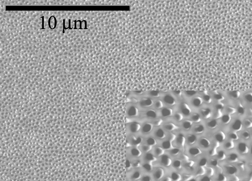
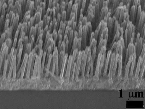
Encapsulation of nanowires within an ordered template offers the possibility of manipulating nanowires into useful configurations and allows their aspect ratios and, hence, their physical properties to be tailored. Anodic aluminum oxide (AAO) templates have cylindrical pore geometry with diameters between 10 – 200 nm in diameter and can also be arranged in uniform hexagonal arrays. The inclusion of material inside the pores is similar to growth within lithographically defined regions utilized in current device fabrication. We have been using these templates for nanomaterial synthesis, providing an architecture to prepare high-density nanowire arrays.
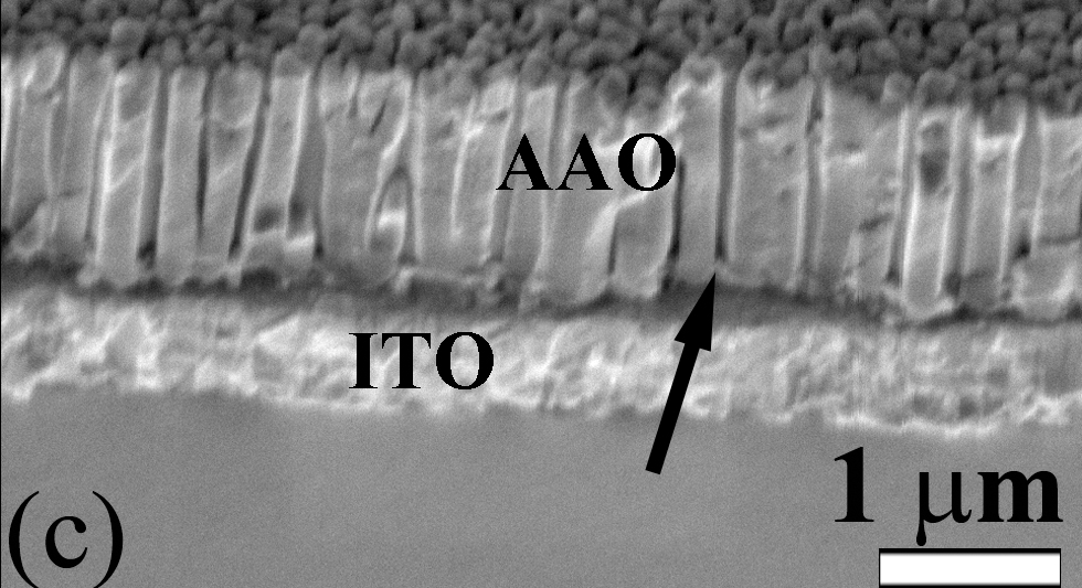
The ability to control the template structure enables the systematic study of nanowire array properties on the photoactive surface area and charge transport of nanowire-based dye-sensitized solar cells (DSSCs). One of the key technological steps in making these devices is to anodize aluminum directly onto ITO conductive glass substrates. This intimate contact enables epitaxial growth of nanowire arrays and provides direct electrical contact to the nanowires synthesized within the pores. Although the anodization of aluminum on ITO has been established, the film often delaminates because of the large expansion during oxidation. However, an adhesion interlayer enables the formation of porous, transparent films.
|
|
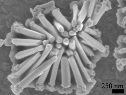
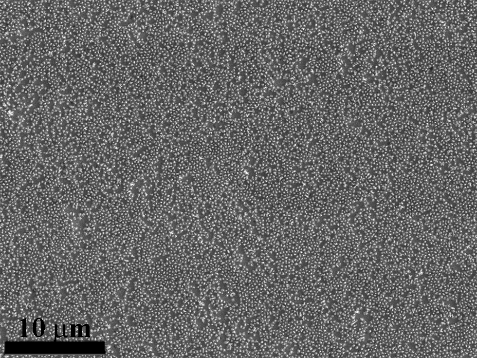
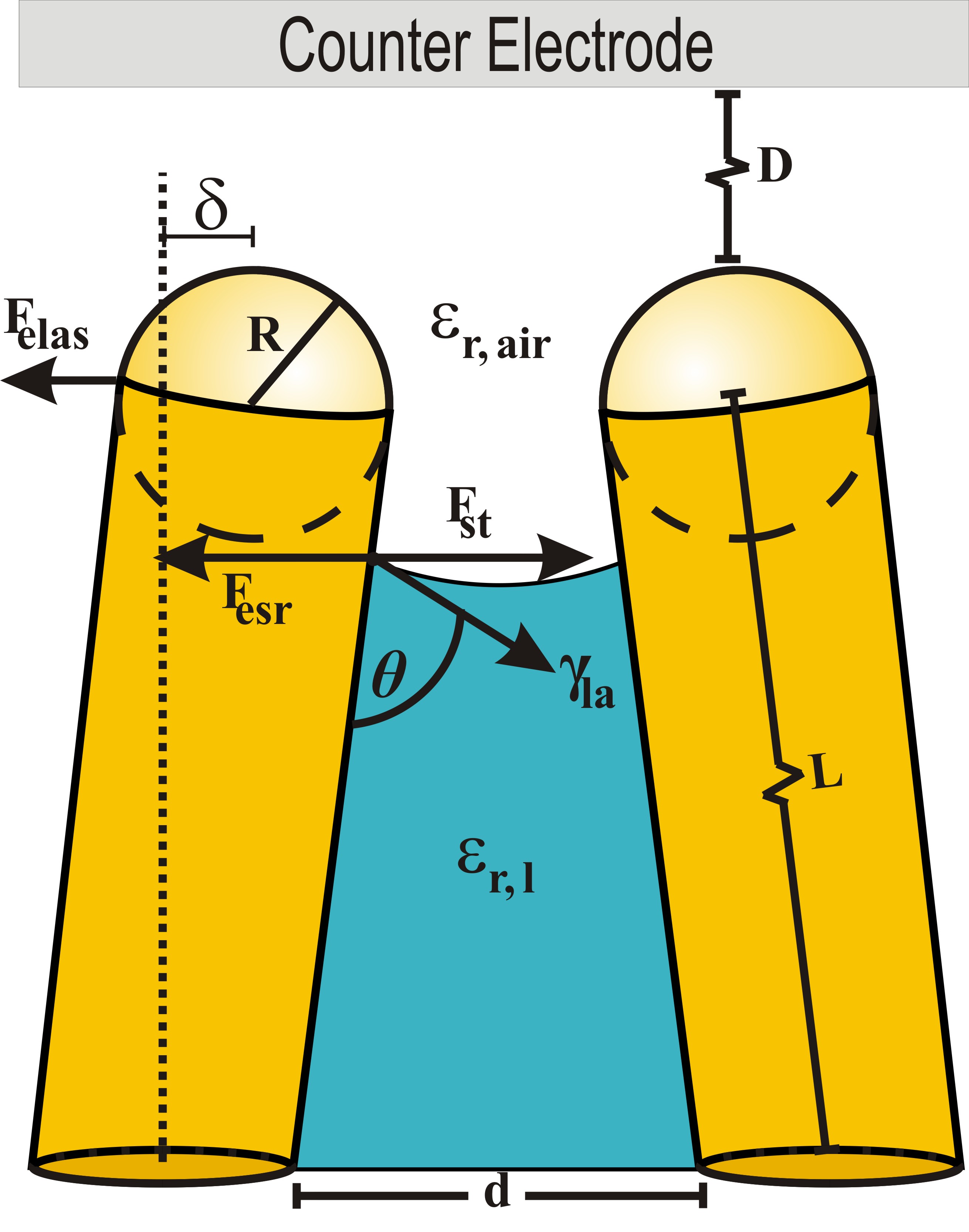 NaOH and phosphoric acid have been effective at liberating nanowires from AAO. However, drying the nanowire array often leads to aggregation in high-density arrays because of the substanital forces from surface tension acting on each nanowire. The inability to control the surface tension has traditionally limited nanowires to shorter than a few microns or required critical point drying. We have developed a simple technique to eliminate these aggregation effects using electric fields. A voltage supply is applied to the nanowire array causing electrostatic charge on the nanowire tips. This charge provides significant electrostatic repulsion once the nanowires are pulled close to each other by the forces due to surface tension. NaOH and phosphoric acid have been effective at liberating nanowires from AAO. However, drying the nanowire array often leads to aggregation in high-density arrays because of the substanital forces from surface tension acting on each nanowire. The inability to control the surface tension has traditionally limited nanowires to shorter than a few microns or required critical point drying. We have developed a simple technique to eliminate these aggregation effects using electric fields. A voltage supply is applied to the nanowire array causing electrostatic charge on the nanowire tips. This charge provides significant electrostatic repulsion once the nanowires are pulled close to each other by the forces due to surface tension.
|
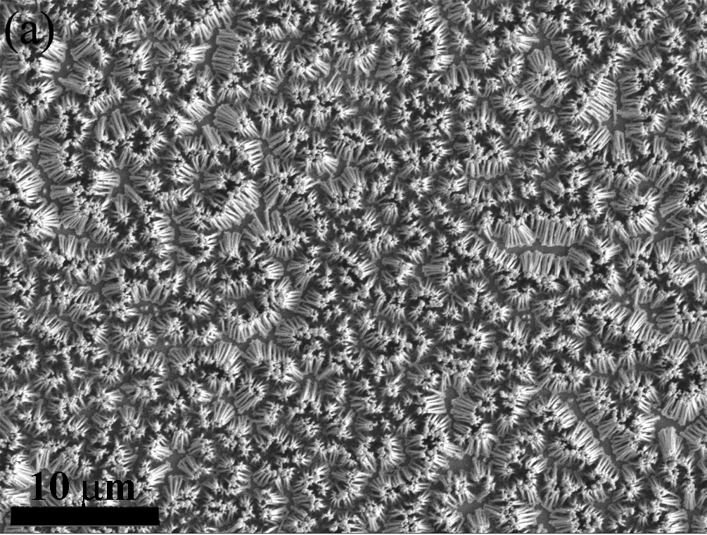 
Aggregated Nanowire Array |
Non-Aggregated Nanowire Array |
Related Publications
J.J. Hill, K. Haller, B. Gelfand, and K.J. Ziegler. Eliminating Capillary Coalescence of Nanowire Arrays with Applied Electric Fields. ACS Appl. Mater. Inter. 2010, 2, 1992. [link]
J.J. Hill, K. Haller, and K.J. Ziegler. Direct Fabrication of High-Aspect Ratio Anodic Aluminum Oxide with Continuous Pores on Conductive Glass. J. Electrochem. Soc. 2011, 158, E1. [link]
J.J. Hill, S.P. Cotton, and K.J. Ziegler. Alignment and Morphology Control of Ordered Mesoporous Silicas in Anodic Aluminum Oxide Channels by Electrophoretic Deposition. Chem. Mater. 2009, 21, 1841. [link]
K.J. Ziegler, B. Polyakov, J.S. Kulkarni, T.A. Crowley, K.M. Ryan, M.A. Morris, D. Erts, and J.D. Holmes. Conductive films of ordered nanowire arrays. J. Mater. Chem. 2004, 14, 585. [link]
 Nanowire Arrays